

2025 VLSI Technology Forum - Advanced Substrate for High Performance Heterogeneous Integration
Original Article by SemiVision Research (IEEE , ITRI ,VLSI TSA ,Ibiden ,Unimicron ,Ajinomoto , Nvidia)

With support from the Department of Industrial Technology, Ministry of Economic Affairs, the Industrial Technology Research Institute (ITRI) hosted the 42nd International Symposium on VLSI Technology, Systems and Applications (VLSI TSA) 2025, one of the most prominent annual semiconductor events.
Drawing participation from over a thousand industry professionals, this year's symposium focused on AI-driven semiconductor innovation.
Attendees emphasized that Taiwan possesses strong capabilities in advanced packaging and chip manufacturing, and should continue to strengthen its positioning in heterogeneous integration, advanced transistor development, and system-level integration.
By enhancing its manufacturing and system integration leadership and deepening international collaboration, Taiwan can secure its critical global position in AI and high-performance computing (HPC) applications, laying a solid foundation for future semiconductor advancement.

Dr. Shih-Chieh Chang, VLSI TSA Conference Chair and General Director of ITRI’s Electronic and Optoelectronic System Research Laboratories, noted that this year’s symposium convened top global experts in semiconductors and AI.
Key topics included advanced logic transistor architectures, back-side power delivery networks (BSPDN), heterogeneous integration, die-to-die interconnects, and co-packaged optics (CPO)—all pivotal breakthroughs to enhance AI chip performance and energy efficiency. These trends demonstrate the forward-looking direction and R&D competitiveness of the semiconductor industry.
Against the backdrop of global geopolitical shifts and supply chain restructuring, Taiwan plays a crucial role as a trusted hub in the democratic semiconductor supply chain. It continues to forge resilient, high-tech partnerships with like-minded nations through technological innovation and international collaboration.
Meanwhile, the rapid adoption of AI technologies has brought forth an urgent talent shortage. To address this challenge, the industry must foster cross-disciplinary integration, deepen industry-academia collaboration, and increase R&D investment to build a comprehensive talent development ecosystem for AI and semiconductors—reinforcing Taiwan’s competitiveness in the global technology arena.

Building on this momentum, advanced packaging technologies have become increasingly critical in chip manufacturing, especially in the domains of servers and high-performance computing (HPC), where they play a pivotal role in boosting performance while reducing power consumption.


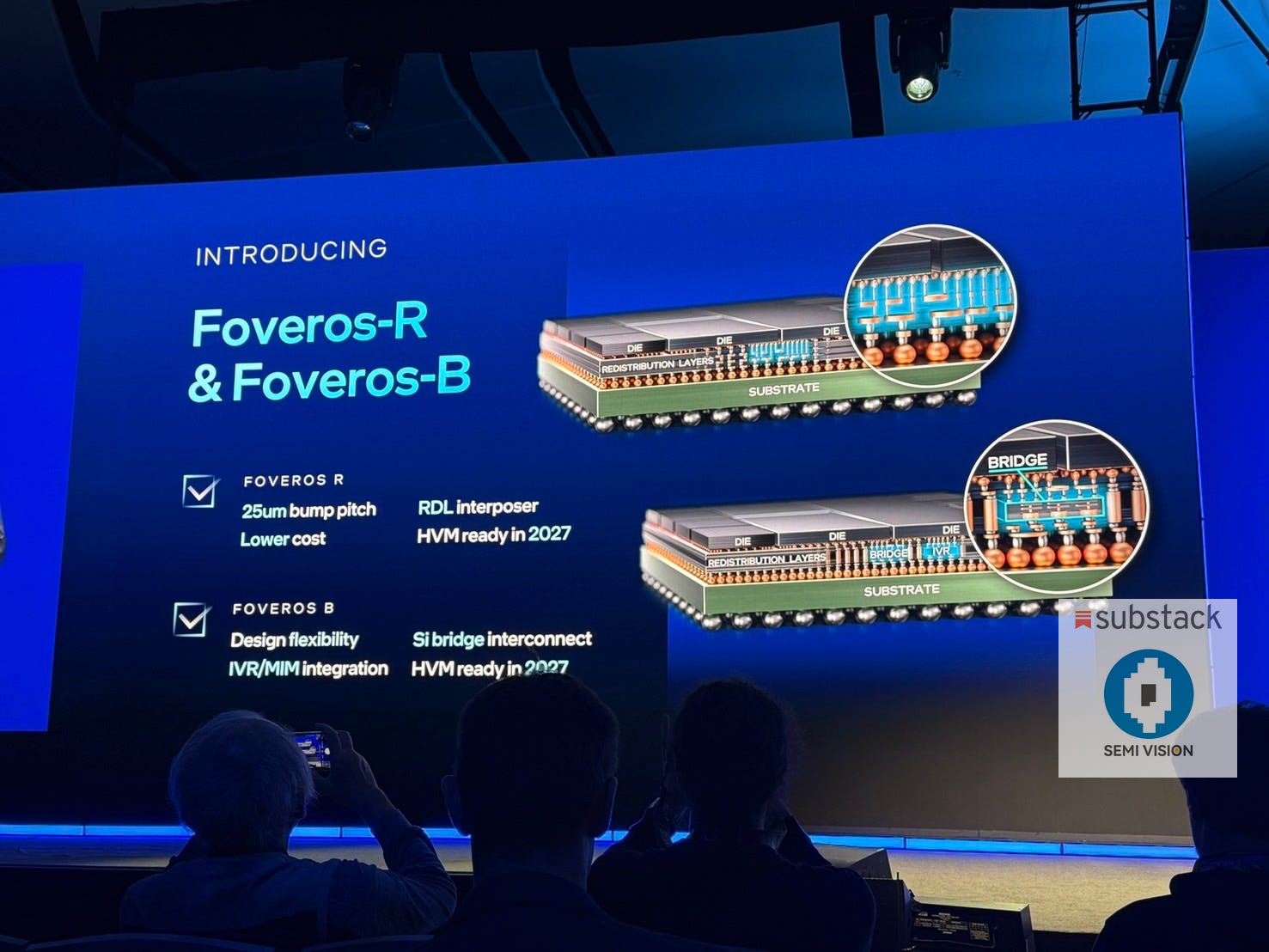
Semiconductor giants such as TSMC and Intel are actively developing various advanced packaging platforms to meet these demands. TSMC’s CoWoS (Chip-on-Wafer-on-Substrate) and Intel’s EMIB (Embedded Multi-die Interconnect Bridge) and Foveros 3D packaging technologies exemplify this global race toward more efficient integration of compute, memory, and I/O components.

At the heart of these technologies lies the substrate, which serves not only as a mechanical foundation but also as a high-density interconnect platform that ensures signal integrity, power delivery, and thermal management. As packaging complexity increases—through chiplet architectures, 2.5D/3D integration, and co-packaged optics—the performance and reliability of the substrate material become mission-critical.
Thus, substrates are no longer passive layers—they are now active enablers of advanced system scaling, making their innovation and manufacturability a central focus for the next generation of semiconductor advancement.
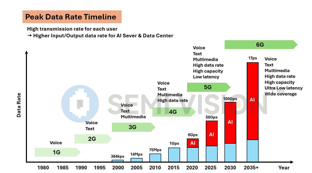
The rapid evolution of peak data rates over time, transitioning from traditional wireless communication generations (1G to 6G) to the emerging data demands of AI systems.
While wireless standards have steadily progressed—from supporting basic voice in 1G to high data rate, low-latency multimedia in 5G and eventually ultra-low latency and wide coverage in 6G—the real inflection point begins around 2020. From this point forward, the data rate requirements driven by AI applications (shown in red) start to rise exponentially.
By 2025, AI systems already require 50 Gbps, growing to 100 Gbps by 2030, and potentially reaching 1 Tbps by 2035. This growth far exceeds the bandwidth needed for conventional mobile communications, as AI workloads involve large-scale model training, real-time inference, multi-modal data processing, and high-bandwidth interconnects across GPUs, memory, and storage.
The chart emphasizes a clear shift: AI is now the primary force pushing data rate demands into the terabit era, requiring next-generation system architectures, interconnect technologies, and packaging innovations to keep up with the accelerating pace of compute and I/O.
For Paid Members, SemiVision will discuss topics on
High Speed Input/Output in Ai chip and PCB
Review Substrate Market Share (Global Players)
Why is substrate manufacturing so heavily centered in Asia?
What Is IC Carrier (IC Substrate)?
Substrate in CoWoS
Ibiden: Technological Advancement and development of IC Package Substrate
Ibiden: IC Substrate Market and Trend
Unimicron: Technology Development Focus and Needs for Advanced Substrate
Ajinomoto Market and Expansion Plan