

Advantest Leading the AI Testing Wave: Earning the Title of the “ASML of the Test Industry”
Original Articles By SemiVision Research (TSMC, Nvidia , Advantest , Teredyne , Formfactor , FiconTEC , Broadcom ,Marvell , MPI)

In the previous article, we discussed many topics related to silicon photonics, advanced packaging, CMOS scaling technology, and some testing concepts. As AI chips become increasingly complex, ensuring chip reliability presents significant challenges. We have also observed the rapid growth of the testing industry. Today, we will briefly talk about the testing leader: Advantest.


Starting with Electronic Measurement Technology: Advantest’s Growth Alongside Japan’s Electronics Industry
Our origins trace back to being a developer and manufacturer of multifunctional electronic measuring instruments, such as voltmeters and frequency counters. After achieving success in this field, we adopted an effective strategy: focusing on niche markets and leveraging advanced technology to deliver high-performance products, thereby securing market share.
As Japan’s electronics industry expanded in the late 1960s, we were among the earliest to foresee the semiconductor industry’s potential to create historic opportunities. We directed our capital investment toward developing testing systems based on our electronic measurement expertise. Overcoming management crises and other challenges, we successfully launched world-class semiconductor test systems.
Milestones
1954 – Founded Takeda Riken Industry Co., Ltd.
1957 – TR-124B digital frequency counter became a best-selling product.
1963 – Introduced Japan’s first domestically produced digital voltmeter with a 100,000-digit display.
1972 – Released Japan’s first domestically produced semiconductor test systems: T-320/20 and T-320/30.
1979 – Launched the world’s highest-performance VLSI test system with a test frequency of 100 MHz.

Advantest’s Rapid Growth Alongside the Semiconductor Industry
During this era, fueled by the rise of personal computers and the emergence of the internet, the semiconductor market expanded significantly. Advantest’s semiconductor testing systems integrated cutting-edge measurement technology with high-volume manufacturing capabilities, supporting the evolution and advancement of semiconductor equipment. By 1985, the company had become a global leader in the semiconductor test equipment market, with testing systems becoming its core business.
Milestones
1982 – Established a local subsidiary in the United States, later expanding manufacturing operations to other regions worldwide.
1985 – Renamed as Advantest Corporation. According to VLSIresearch (now TechInsights), the company ranked No. 1 in global market share for semiconductor test equipment.
1993 – Launched the T6691, a large-scale integrated circuit test system offering industry-leading testing speeds of 500 MHz/1 GHz.
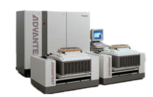
1995 – Introduced the T5581, a 250 MHz S-DRAM memory test system, which became a best-selling product.

T5581, a 250 MHz S-DRAM memory test system
From expanding globally to pioneering high-speed, high-performance testing solutions, Advantest cemented its position as a driving force in advancing semiconductor testing technology.
Advantest’s Alignment with Shifts in Semiconductor Value Chains
At the turn of the 21st century, the rise of smartphones and the proliferation of personal computers became major drivers of semiconductor demand. The global distribution of semiconductor design and manufacturing advanced rapidly, creating a growing need for cost-efficient and high-performance testing. In response, Advantest worked to stabilize its business base while taking proactive, forward-looking measures, including the acquisition of overseas companies.
In 2011, Advantest acquired Verigy, marking the second time in its history that the company’s destiny hinged on a bold strategic move. This acquisition brought significant returns, as Verigy’s global customer base and operational expertise provided a strong foundation for Advantest’s growth in the years to come.
Key Milestones
2000 – Selected as one of the 225 stocks comprising the Nikkei 225 Stock Average.
2001 – Established Japan’s largest bio-cluster within the Gunma R&D Center.
2003 – Acquired Nihon Engineering’s open architecture SoC test system T2000.
2008 – Acquired Credence Systems GmbH.
2011 – Acquired leading semiconductor test equipment company Verigy.
2013 – Acquired W2BI.COM.
2018 – Announced a mid-term business management plan with a broad, long-term vision.
2019 – Acquired Astronics’ semiconductor system-level test business in the U.S.
Through strategic acquisitions, market foresight, and continued technological innovation, Advantest has positioned itself as a global leader, ready to adapt to the evolving semiconductor value chain.
Advantest Expands Business Through Measurement Technology While Driving ESG Sustainability
Advantest anticipates that the widespread adoption of AI and 5G will trigger explosive growth in global data processing demands, ushering the semiconductor market into a new stage of development. Semiconductors play an increasingly critical role in powering today’s data-driven society, where precision, complexity, and capacity requirements continue to rise—along with the need for greater reliability.
As digital transformation accelerates and the semiconductor value chain continues to evolve and expand, Advantest remains committed to creating new value for customers. This includes broadening its business scope into system-level testing and data analytics.
Key Milestones
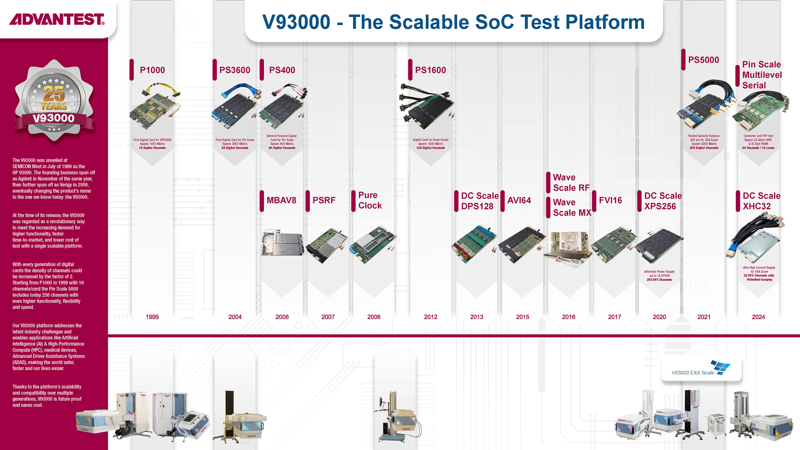
2020 – Acquired U.S.-based Essai Inc. and formed a business alliance with PDF Solutions (U.S.); launched the V93000 EXA Scale™.
2021 – Established an ESG Action Plan, announced the second Mid-Term Management Plan, and acquired U.S.-based R&D Altanova Inc.
2022 – Acquired CREA S.r.l. in Italy.
2023 – Acquired Taiwan-based ACE Technology Co., Ltd.
With these strategic moves, Advantest strengthens its global presence while reinforcing its commitment to sustainable growth and environmental, social, and governance (ESG) principles.
Advantest Leading the AI Testing Wave: Earning the Title of the “ASML of the Test Industry”
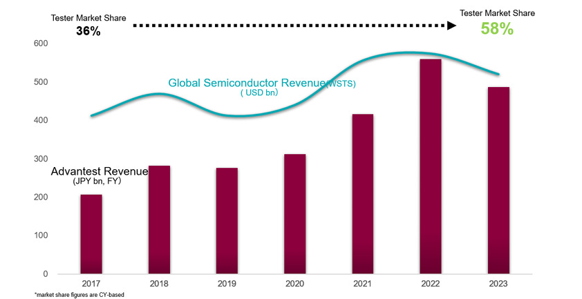
Global Positioning and Market Leadership
Advantest (Japan) is the world’s leading supplier of Automated Test Equipment (ATE), holding roughly 50% of the global market share in 2023, with the combined share of Advantest and the U.S. player Teradyne reaching around 80%. The company offers a comprehensive product portfolio that spans SoC, mixed-signal, and memory testers, system-level test (SLT) platforms, test handlers, and interface solutions, all integrated with edge computing and data analytics capabilities.
AI and HPC Testing Strategy
Advantest is aggressively investing in AI and high-performance computing (HPC) chip testing, recognizing that next-generation processors and accelerators demand more complex validation methodologies. Its flagship V93000 EXA Scale platform and T2000/7038 SLT series are specifically engineered to handle high current loads, high-speed serial interfaces, and advanced system-level testing. These platforms are complemented by the Advantest Cloud Solutions (ACS) ecosystem, which leverages AI and machine learning for real-time analytics and adaptive test decision-making.
Industry Impact and Technology Leadership
The company has frequently highlighted “AI chip testing” as a strategic theme at multiple international conferences, signaling its determination to lead the emerging AI/HPC testing domain. By offering cutting-edge, highly automated, and data-driven test solutions, Advantest positions itself as the “ASML of the test industry”—an indispensable enabler for the semiconductor ecosystem, especially as AI workloads and chip complexity accelerate.

Teradyne (United States)
Holding approximately 30% of the global ATE market, Teradyne is a key competitor in semiconductor test solutions. Its core product lines include the UltraFLEX and J750 SoC test systems, as well as memory test platforms, and the company also has a presence in the industrial robotics sector.
Teradyne has expanded its capabilities in RF and system-level testing through acquisitions such as LitePoint(wireless and RF test solutions) and Eagle Test Systems (high-speed and analog test technologies). The company’s CEO has emphasized that AI chips are expected to drive revenue growth in the second half of the year, underscoring the significant impact of the AI boom on semiconductor test demand.
Cohu (United States)
Cohu focuses on power and RF (radio frequency) testing, with its product portfolio integrating burn-in and system-level testing (SLT) capabilities through the Island platform. The company has also been expanding its robotics and thermal management technologies to meet the requirements of power semiconductors and AI chip testing, where precise handling and high-temperature operation are critical.
While Cohu continues to enhance its presence in specialized and high-growth markets, its overall scale remains smaller than industry leaders Advantest and Teradyne, positioning it as a niche player targeting the evolving demands of AI and power semiconductor testing.
NI (National Instruments, post-merger with Texas Instruments and Emerson)
NI provides modular and flexible test platforms that cater to a wide range of semiconductor and electronic system validation needs. Following its 2024 merger with Emerson, the company expanded its footprint into the Industrial Internet of Things (IIoT) and edge analytics domains, aiming to bridge industrial automation with advanced test solutions.
In 2025, Advantest and Emerson announced a strategic collaboration to build an AI-driven test ecosystem, combining Emerson’s industrial edge computing capabilities with Advantest’s real-time data and analytics platforms. This integration is designed to enhance semiconductor test efficiency, improve yield, and enable adaptive, data-driven test workflows, reinforcing NI’s role as a key enabler in the era of AI-powered semiconductor manufacturing.
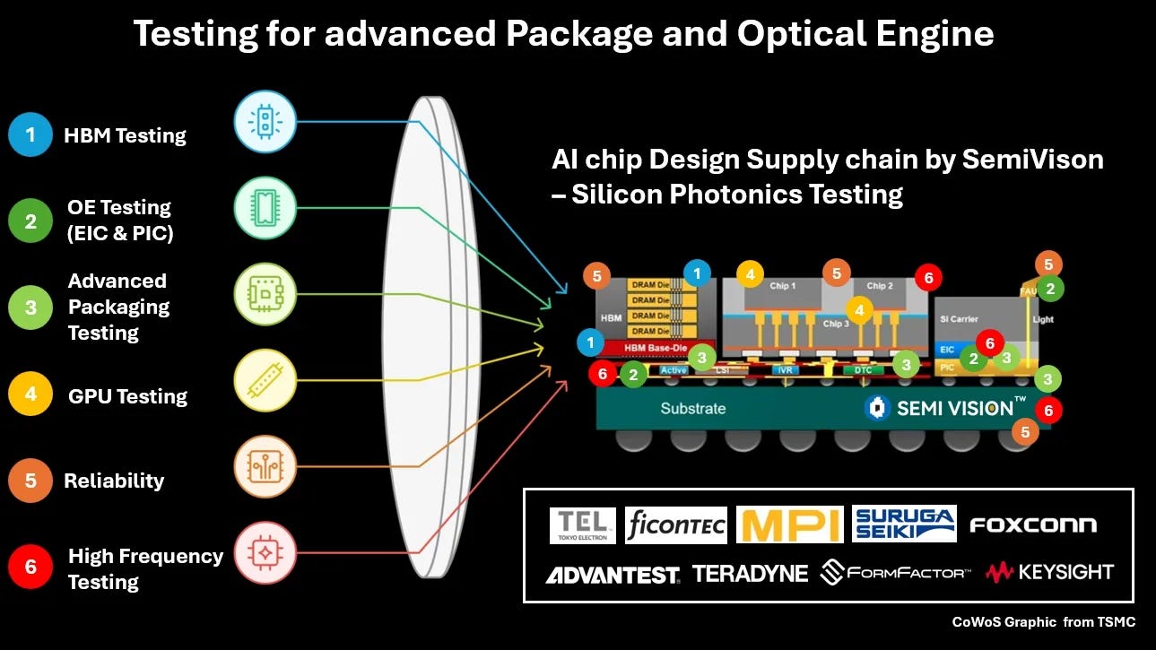
In addition to equipment suppliers, probe card companies such as FormFactor have formed alliances with Advantest, providing high-density probe and test solutions for silicon photonics and 2.5D/3D packaging.
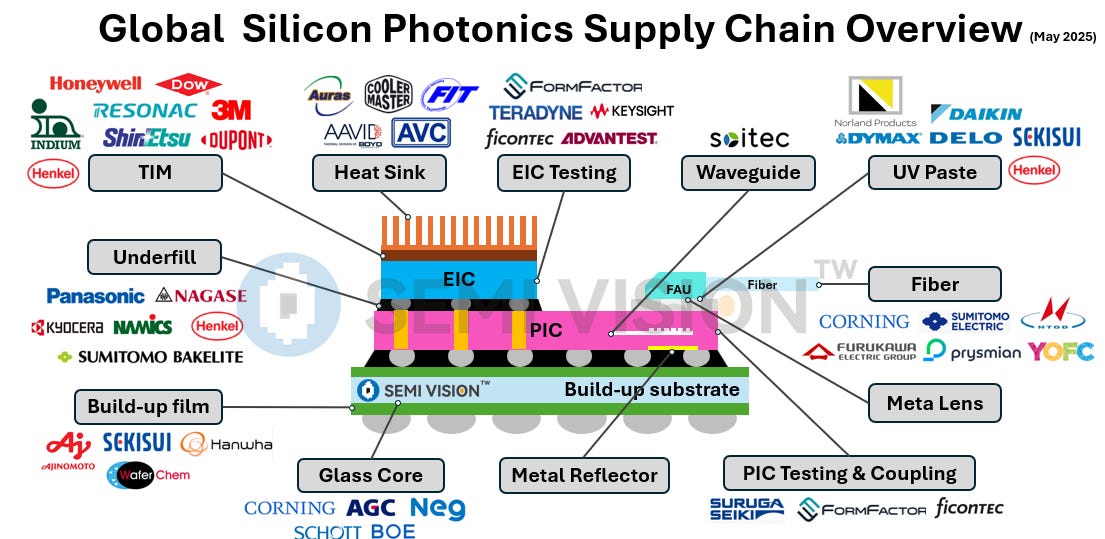
For silicon photonics solutions, we currently see ficonTEC, MPI, and Suruga Seiki offering corresponding systems, with double‑side testing technology as the key focus for all of them.
As AI chips continue to grow in size and power consumption, test times inevitably increase, while reliability remains a non-negotiable priority. To ensure stable performance in real-world applications, the industry widely adopts burn-in testing, which applies high-temperature and high-voltage accelerated stress conditions to induce early failures in weak components before shipment. This process effectively filters out initial defects corresponding to the early-failure phase of the “bathtub curve,” ensuring the product maintains high reliability throughout its operational lifetime.
For Paid Members , SemiVision will discuss topics on
AI and HPC Driving a New Era in Semiconductor Testing: From ATE to SLT in Technology Evolution and Market Growth
Importance of Burn-In Testing
Reasons for Longer Burn-In Times in AI Chips
Testing’s Background and Industry Overview
Current Development Progress and Public Information
High-Density and Double-Side Testing Solutions for Silicon Photonics: A Comparative Overview of FormFactor, ficonTEC, and MPI
1. FormFactor × Advantest Alliance
2. ficonTEC × Teradyne Dual-Side Testing Solution
3. MPI – Multi-Function Silicon Photonics Probing Systems
Market Trends and Industry Applications
Future Impact and Potential Opportunities
Technical Principles and Testing Challenges
Market Trends and Application Scenarios
The Duel of the Test Giants: Advantest vs. Teradyne in the High-Speed Interface Race
New Opportunities for Taiwanese Manufacturers: The Future Outlook for Probe Cards, Fixtures, and ATE Component Supply Chains
Exchange Rates, High Base, and Technology Upgrades: Where Are Advantest’s Challenges and Opportunities in 2025?
Layered Test Architecture: A Blue Ocean Strategy for AI Packaging Testing from Wafer to Module
Taiwanese ATE Makers Aim for Transformation: From Component Supply to Full System ODM – Who Will Break Through?
Advantest’s Silicon Photonics Strategy: Focused on Photonic Chip and Advanced Packaging Test Platforms
