

Unlocking Precision at Scale: TSMC’s Vision for AI and HPC Test
Original Articles By SemiVision Research (IEEE ECTC , SWTest , TSMC , Teradyne , ADVANTEST , FormFactor, FiconTEC ,Surugaseiki, Nvidia, Broadcom , Marvell)

TSMC, for the first time, has addressed the Test Challenges in the HPC and AI Era, presenting valuable insights.
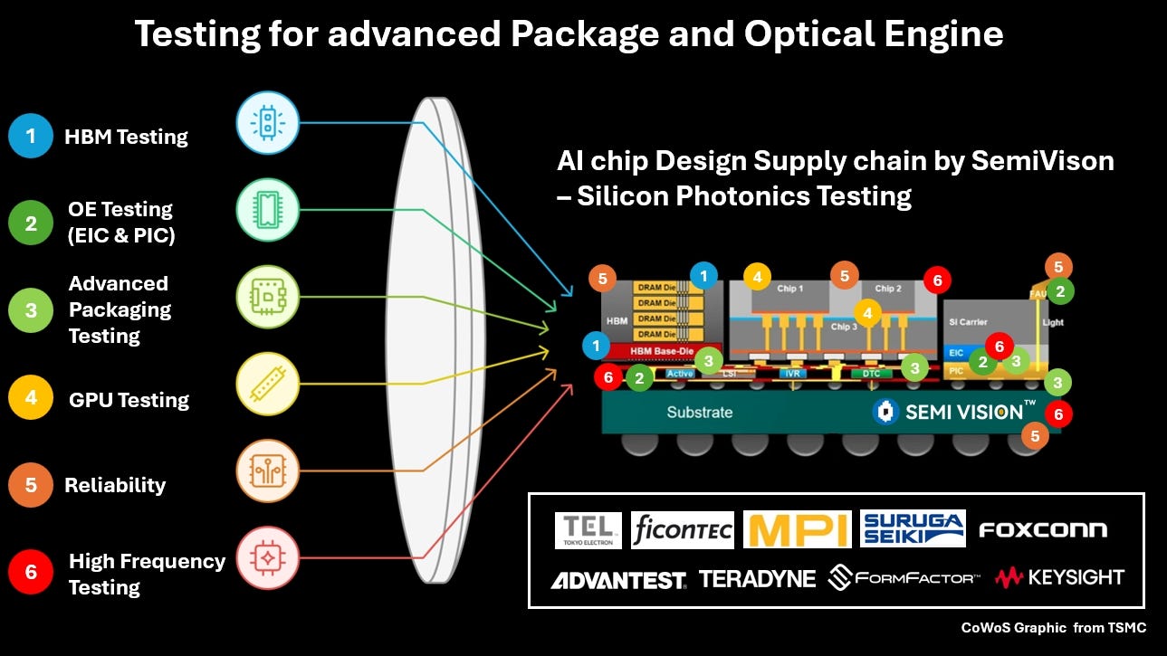
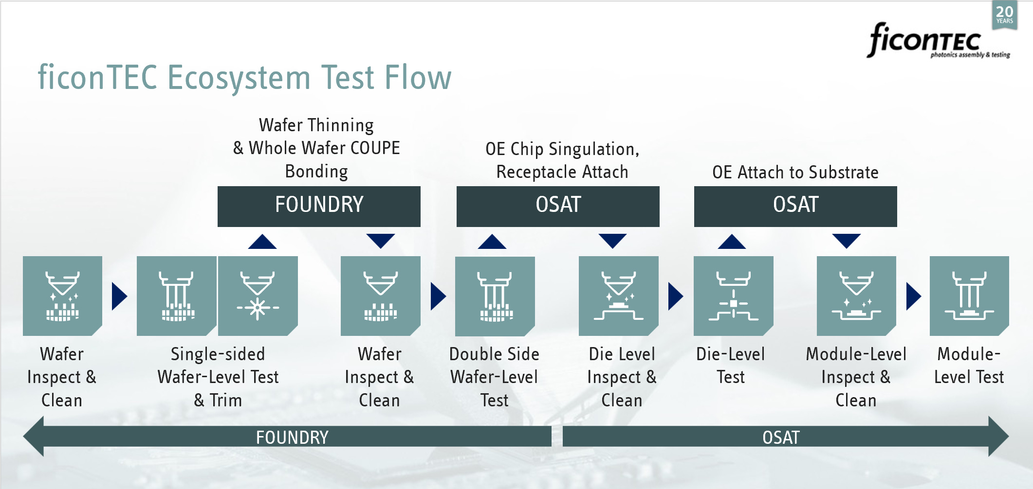
This presentation covers the process flow of CoWoS and PIC/EIC Optical Engines, which is highly important information that every reader and supply chain partner interested in learning about testing must understand.
CPO Testing Process is a critical concept, as it is essential to address how to measure PIC (Photonic Integrated Circuit), EIC (Electronic Integrated Circuit), and even the Optical Engine (OE). These topics are definitely worth discussing in depth.
The semiconductor industry is undergoing a deep transformation—one that challenges not only the physical structure of chips, but also the entire logic of how we test them.
In this post-Moore era, defined by AI chips, chiplets, HBM, and co-packaged optics (CPO), we are no longer simply chasing higher performance or transistor density. We are confronting a far more practical, pressing, and critical question: How do we test these extremely complex chips and systems?
This isn’t just an engineering problem—it’s a value chain problem. Because when testing fails, it’s not just a chip that gets scrapped—it’s the entire module, the entire packaging layer, sometimes even a multimillion-dollar AI system that crashes. And the risks begin at the wafer stage, carry through packaging and integration, and culminate in final system-level testing. Every step is a potential point of failure.
You may not have noticed, but in this world obsessed with generative AI and trillion-parameter models, the compute we rely on is actually built upon invisible foundations—the testing infrastructure that ensures everything works as intended.
That’s why it’s time to rethink what we consider “core value” in the semiconductor industry.
For years, we’ve focused on design, process nodes, yield, and packaging—while treating testing as a supporting or even secondary activity. But that paradigm no longer holds. When a chip disaggregates into ten or more chiplets, when HBM becomes not just a memory module but a compute-enabled element, when lasers and optical engines are co-packaged with ASICs—traditional testing methods simply fall apart.
And if we continue looking at this industry with yesterday’s lens, we’ll fail to understand why test equipment is now among the fastest-growing categories of capital expenditure. We won’t comprehend why TSMC is publicly highlighting topics like probe card design, FAU alignment, anti-vibration platforms, or double-sided probing. And we certainly won’t understand how a company like ficonTEC—once known primarily for optical assembly—is now positioned at the heart of scalable CPO production.
It’s not just that testing has become harder. Testing has become the center of value.
Let’s bring it down to specifics.
Testing AI chips isn’t just about speed—it’s about thermal management, high-frequency signal integrity, contact density, and probe durability. With chips requiring thousands of pins, each carrying up to 1A of current, and thermal loads exceeding tens of watts, testing platforms are pushed to their mechanical and thermal limits. If you can’t test it accurately, you can’t ship it. And if you can’t ship it, you risk system-wide failures, customer returns, brand damage—or losing entire AI cluster orders.
You might think memory is simpler—but not anymore. As HBM stacks begin incorporating logic dies—controllers, processors, and even embedded compute—quality can no longer be judged on a memory-only basis. With the emergence of custom HBM architectures, traditional DRAM testing falls short. New strategies must test memory and logic in tandem.
Now consider silicon photonics and CPO. From a single PIC die to EIC integration, to FAU attachment, to a fully integrated CPO module—this isn’t just a packaging problem. It’s a testing problem. How do you ensure optical alignment remains precise even under vibration? How do you perform double-sided electro-optical probing? Can your test platform support both grating couplers and edge couplers on the same station? If not, your throughput won’t scale to meet the demands of the AI era.
These aren’t hypothetical engineering puzzles. These are very real, very urgent questions being asked by NVIDIA, Intel, TSMC, and Samsung as they prepare next-generation platforms for hyperscalers and global customers.
The answers lie in testing.
Over the next sections, we’ll dig into these frontline challenges:
– The extreme probe card requirements of AI chips
– KGD strategies for HBM before packaging
– Double-sided alignment for SiPh wafer testing
– Stability in optical engine assembly
– The value of RWAT, WLCP, and AST for early defect screening
And more importantly, we’ll expose the players who are winning in this new testing economy.
Why TEL’s wafer prober is becoming the entry ticket for AI chip testing.
Why Advantest continues to expand its footprint in the HBM test market.
Why FormFactor’s high-frequency probe cards and optical alignment platforms are being adopted across the global CPO ecosystem.
Why MPI is carving out a strong position in photonic test.
Why ficonTEC’s evolution from assembly automation to the heart of CPO test platforms is a journey no one in the industry can ignore.

And why Suruga Seiki is becoming a foundational enabler in establishing the precision alignment ecosystem for silicon photonics testing—bridging wafer-level and module-level stages with nano-scale mechanical stages, optical benches, and active alignment systems that now serve not only research labs but also production environments for PIC-based systems.
Furthermore, Foxconn Research Institute is quietly but steadily investing in the next wave of silicon photonics innovation—developing modular photonic engines and pioneering materials platforms such as Lithium Niobate on Insulator (TFLN), electro-optic polymers, and Silicon-Organic Hybrid (SOH) integration. These efforts are not only expanding Foxconn’s presence in data center optics and AI infrastructure, but also positioning it as a strategic player in the convergence of photonics and advanced packaging at scale.
From wafer probing to AI-centric optical modules, these players are rewriting the rules of the test and measurement domain—and reshaping the foundations of the next generation AI infrastructure.
This is not just a new chapter in testing.
This is the new logic of value.
Behind all of this lies a profound transformation—one that is redefining what constitutes core competitiveness in the semiconductor industry. And at the heart of this transformation, it’s no longer about process nodes, design IP, or even advanced packaging materials. It’s about this simple truth: Who can test chips more accurately, more efficiently, and more comprehensively.
This is the new battleground. And the content you’re reading now is your invitation into its deepest waters.
Testing is no longer a verification step—it is the value itself.
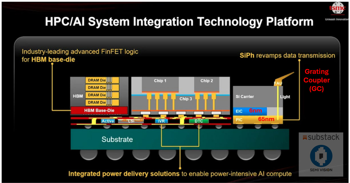
When we revisit the system integration platform diagram, we cannot just fixate on familiar keywords like HBM, GPU, or Optical Engine. While these are undoubtedly the hotspots of advanced packaging, if we aim to truly grasp the essence and complexity of system-level integration, testing and reliability validation emerge as the most overlooked, yet most decisive factors for yield and manufacturability.
In this integration platform presented by TSMC, we can identify three major technological vectors:
Vertical stacking of high-bandwidth memory (HBM) and logic;
Horizontal chiplet integration across a multi-die system;
Incorporation of a silicon photonics (SiPh) platform to enable next-generation optical interconnects.


However, each of these domains—regardless of how cutting-edge they are—requires a rigorous, layered, and well-orchestrated testing strategy to become viable products.
Take HBM for example: testing isn’t just about validating individual DRAM dies. It involves validating the full stack along with the logic base-die. That means checking TSV conductivity, thermomechanical stress integrity, and power-sequencing stability under real-world load conditions. This class of testing demands high-speed probing stations and integrated thermal test systems, where leading suppliers like Teradyne, Advantest, and FormFactor dominate. Increasingly, these companies are deploying AI-driven adaptive test platforms, capable of real-time optimization during test execution.
Now consider the central logic die. Testing here is even more demanding. With embedded IVRs (Integrated Voltage Regulators), advanced PDNs, low-loss SerDes (112G/224G), and digital control blocks all operating in harmony, traditional scan and BIST strategies fall short. Instead, test frameworks must integrate DFT-aware simulations, high-speed signal feedback systems, and monitor elements like Built-In Monitoring (BIM) across multi-layer RDLs. These are not accessories—they’re foundational to the new testing architecture.
The most complex layer, however, lies in Optical Engine Testing. This involves not only validating the co-functionality of EICs (Electronic ICs) and PICs (Photonic ICs), but also measuring the physical integrity of the optical path: insertion loss, coupling efficiency, return loss, and ultra-precise fiber-to-chip alignment via Grating Couplers (GC) or Edge Couplers. Traditional electrical ATE platforms are not equipped to handle this. Instead, purpose-built systems from vendors like ficonTEC, MPI, and EXFO offer dual-sided wafer probing, six-axis optical alignment, optical power metrology, BER analysis, and adaptive coupling scan functionality.
Importantly, these tests don’t stop at the point of measurement—they extend into reliability qualification. This includes thermal cycling (TCT), humidity testing (HAST), high-temperature storage (HTS), and mechanical stress simulations (drop, vibration, etc.). When optical engines are co-packaged with bare logic dies, even the mismatch in coefficient of thermal expansion (CTE) becomes a system-level reliability threat. Internal stress distributions during thermal shifts can directly destabilize optical performance and lifetime.
From HBM, to chiplets, to SiPh modules—each component demands a full-stack test strategy and validation flow. Without this layer of systems engineering, even the most advanced packaging and materials cannot be translated into real-world, volume-production success. Going forward, system integration is no longer just about design and packaging—it’s about Test & Qualification Co-Design becoming part of the engineering flow from day one.
In our upcoming SemiVision deep-dives, we’ll be covering:
Strategic roadmaps of leading test equipment vendors
New challenges in HBM 4 and 4E testing
Optical coupling and metrology breakthroughs in SiPh modules
The evolution of reliability qualification standards for system-in-package (SiP) platforms
Stay tuned—because in this era, those who understand testing, understand the future.
For Paid Members, SemiVision will discuss topics on
Advanced Package Testing(HBM, Chiplet, Optical Engine,Full Module)
Key Testing Strategies for Chiplet Systems: The Value and Implementation of Distributed Inline Testing
Probing Test Challenges and Technologies: A Critical Pillar in the Era of Advanced Packaging
The New Frontier of Advanced Testing: Why TSMC Is Talking About “Thermal Challenges”
Thermal Performance: Wafer-Based vs. Singulated Die Testing
Test Challenges and Systematic Strategies in the Era of Advanced Packaging: A Full-Chain Test Approach from HBM to CPO
Four Key Challenges and Technical Barriers in Mass Production Testing of Silicon Photonics (SiPh)
TSMC’s Strategic Approach to Silicon Photonics Testing
AI-Driven End-to-End Test Chain Transformation
AI/ML-Driven DFT and Test Optimization: Ushering in the Intelligent Era of Semiconductor Testing
Test Equipment Vendors and Market Opportunities
