

How Do Advanced Packaging Equipment Vendors Tackle Challenges in a Globalized Market?
Original Article by SemiVision Research (TSMC,UMC,Samsung,Intel,ASML,AMAT, Lam,TEL,KLA,ASE,Amkor,JCET,Disco,Besi ,ASMPT,K&S,Semes,Hanmi,Hanwha, EVG,SUSS,Teradyne,SCREEN,Canon,Nikon,Lasertec)

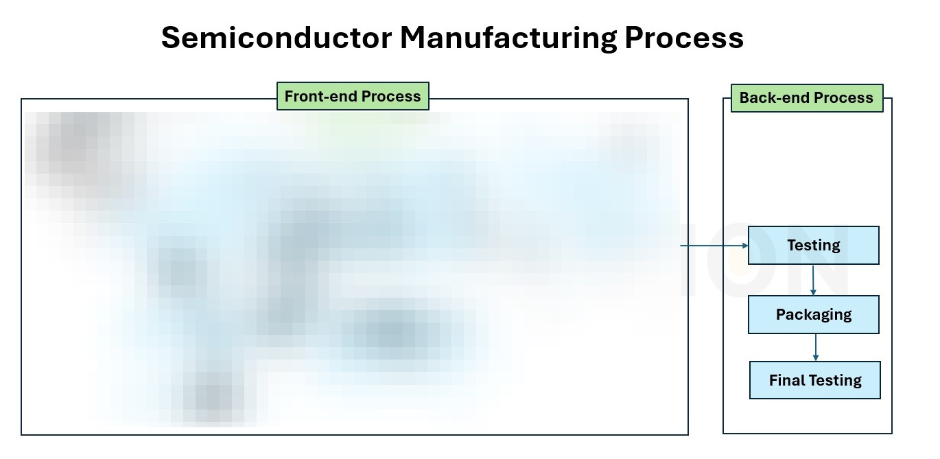
Global Semiconductor Foundries: Front-End WFE and Back-End Packaging Supply Chain Analysis – Facing Globalization Challenges
The race for advanced process nodes has made Wafer Fab Equipment (WFE) in the front-end, as well as back-end packaging equipment, increasingly critical for semiconductor foundries. Leading players such as TSMC, UMC, Samsung Electronics, and Intel control the world’s most advanced process technologies, yet they remain highly dependent on a globalized ecosystem of equipment and materials suppliers. Entering the AI and high-performance computing (HPC) era, demand for advanced packaging platforms—including 2.5D/3D packaging, Hybrid Bonding, and CoWoS—is surging, reshaping the back-end equipment landscape. This paper analyzes the core elements of both WFE and back-end packaging supply chains, while exploring how equipment vendors are responding to the challenges of geopolitics and globalization.
As Moore’s Law slows, advanced packaging has emerged as the key pathway to sustaining semiconductor performance gains. Technologies such as 2.5D/3D packaging, heterogeneous integration, Hybrid Bonding, high-density substrates, and chip stacking not only test equipment suppliers’ capabilities in precision, yield, and material integration but also place them at the center of a complex global market environment. On one hand, equipment vendors must meet the stringent demands of top-tier foundries like TSMC, Samsung, and Intel for next-generation packaging. On the other, they must adapt to geopolitical pressures, government-driven semiconductor self-sufficiency policies, and supply chain diversification trends. Striking a balance between technological breakthroughs and fragmented markets will determine whether advanced packaging equipment suppliers can maintain leadership on the global stage.

In the global semiconductor supply chain, the front-end WFE (Wafer Fab Equipment) and back-end advanced packaging supply chains are increasingly characterized by a dual dynamic of “technological concentration” and “geographic diversification.”
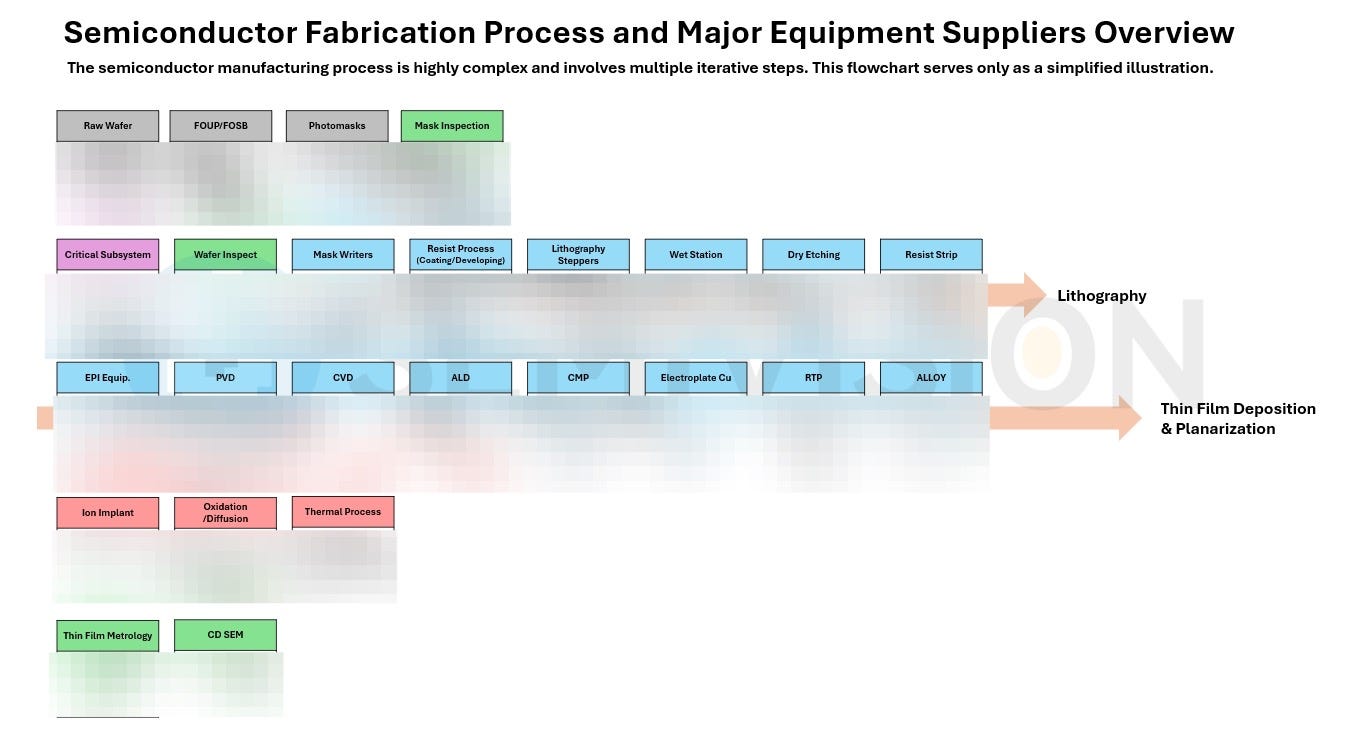
In front-end wafer manufacturing, the sector is almost monopolized by five major players—ASML, Applied Materials, Lam Research, Tokyo Electron (TEL), and KLA—on which foundries such as TSMC, Samsung, Intel, and UMC are highly dependent. While U.S. and Dutch firms remain global leaders in lithography, deposition, and etching, export controls and policies such as the CHIPS Act and the European Chips Act have compelled equipment suppliers to adjust their footprints, establishing new production and service bases across North America, Europe, Japan, and Southeast Asia to strengthen supply chain resilience. Meanwhile, although China’s domestic equipment vendors are rapidly catching up, they currently satisfy less than 14% of back-end demand, making it difficult in the short term to challenge the dominance of international giants.
In the back-end packaging domain, the rise of AI and HPC applications has pushed 2.5D/3D packaging, Hybrid Bonding, and TCB (Thermal Compression Bonding) into the spotlight. The OSAT market is dominated by ASE, Amkor, and JCET, while Disco, Besi, ASMPT, K&S, and Semes form the backbone of the equipment supply chain. For TSMC, CoWoS and SoIC have become critical platforms for driving HPC packaging, which in turn has spurred the development of new materials and technologies such as glass substrates and Hybrid Bonding. Looking forward, as reticle size limitations create bottlenecks, SoW (System-on-Wafer) and CoPoS (Chip-on-Panel-on-Substrate) are expected to gradually replace traditional CoWoS, with glass substrates potentially emerging as the next breakthrough. In this environment, equipment suppliers not only face cost and pricing pressures but must also address challenges related to sustainability, customization, and global competition. Only through technological innovation, product diversification, localized investment, and cross-border collaboration can they maintain leadership and seize the next wave of growth.

In the semiconductor industry, advanced logic processes will remain concentrated among a few dominant players, but advanced packaging opens the door for niche companies with specialized technologies to emerge. At the same time, this shift creates a significant opportunity for specialty chemicals, as it represents a transformation pathway from traditional chemical industries into the semiconductor supply chain. In Taiwan, this localization trend has already given rise to many companies pivoting from conventional chemicals to semiconductor materials, including advanced photoresists, molding compounds, underfills, BARC, and ARC.
We are seeing new innovative materials emerging across CoWoS, HBM, and silicon photonics. Therefore, in the future, the semiconductor industry will need to shift its mindset toward the integration of materials as a core consideration.
While semiconductor supply chain analysis has traditionally focused on equipment, materials are becoming a critical area of discussion. For example:
In the CoWoS supply chain, we see multiple material suppliers involved.
In Optical Engines, UV resins are being used to connect FAUs (Fiber Array Units) and optical modules.
In Hybrid Bonding, specialized adhesives are applied at wafer edges to prevent wafer sliding during wafer-on-wafer (WoW) processes.
In thermal management, the evolution of TIM (Thermal Interface Materials) has introduced new solutions.
This signals a gradual paradigm shift in semiconductors—from equipment-centric to material-centric innovation.
At the upcoming SEMICON Taiwan, numerous equipment vendors are expected to release updates on their latest technologies, illustrating this shift with concrete examples.
SemiVision has compiled a series of important semiconductor suppliers that are well worth exploring. More detailed insights will be prepared and shared with our members.
This article will reference several relevant companies within the semiconductor industry.
TSMC, UMC, Samsung Electronics, Intel, ASML, Applied Materials (AMAT), Lam Research, Tokyo Electron (TEL), KLA, ASE (Advanced Semiconductor Engineering), Amkor, JCET, Disco, Besi (BE Semiconductor Industries), ASMPT (ASM Pacific Technology), Kulicke & Soffa (K&S), Semes, Hanmi, Hanwha, EVG (EV Group), SUSS MicroTec, Teradyne, SCREEN, Canon, Nikon, Lasertec, Kokusai Electric, NAURA, AMEC, Kingsemi, Huaxing, ACM Research, SK hynix, Broadcom, Marvell, Huawei, SMIC, Sony, Denso, Toyota, NVIDIA, Rapidus
For Paid Members, SemiVision will discuss topics on
Future Development Directions of the Semiconductor Industry
Overview of the Front-End WFE Supply Chain
WFE Market Size and Leading Vendors (KE, Lasertec, DISCO, Canon , Nikon, SCREEN, TEL)
Macro Commentary in Semiconductor Industry
Kumamoto’s Second Take-Off: From “Silicon Island” to Semiconductor Revival
Wafer Fab Equipment (WFE) Supply Chain Configuration
Back-End Packaging Equipment and OSAT Supply Chain
Backend Equipment Vendors and Market Share
Advanced Packaging Market Trends and Demand
Supply Chain Strategies in a Globalized Environment
Foundries and OSATs’ Strategies
Impacts and Outlook Amid Globalization Challenges
Global Semiconductor Supply Chain
CoWoS Supply Chain Complexity
Positioning and Limitations of CoWoS
CoWoS Supply Chain and the Rise of Glass Substrates
Interconnection Density as a Packaging Evaluation Metric
SoIC: Capacity and Challenges
Environmental and Sustainability Pressure
Cost and Price Sensitivity in advaced logic node
From Silicon Island to AI Supply Chain
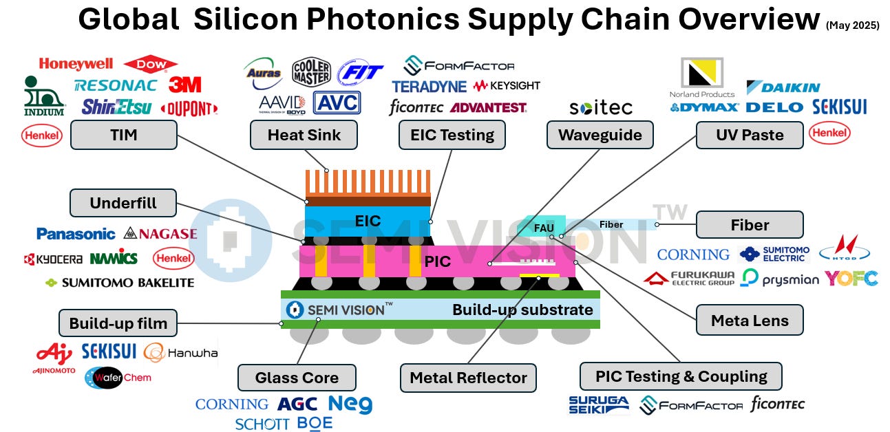
Advanced Packaging and Silicon Photonics Integration
From Copper Interconnects to Optical Interconnects: Materials and Physical Limits
Nonlinear Optics and Material Innovation
