

Intel’s CPO Packaging Roadmap: From Glass Couplers to Pluggable Optical Connectors
Original Article By SemiVision Research [Reading time: 18 mins]


Over five days, DAC provides over 300 technical presentations and sessions that are selected by a committee of electronic design and university research experts offering information on recent developments and trends, management practices and new products, methodologies, and technologies in the electronics industry.
The conference is sponsored by the Association for Computing Machinery (ACM) and the Institute of Electrical and Electronics Engineers (IEEE), and is supported by ACM’s Special Interest Group on Design Automation (SIGDA) and IEEE’s Council on Electronic Design Automation (CEDA).
From Glass Couplers to Pluggable Optical Connectors: A Review of Two Intel Papers on CPO Optical Coupling Packaging Technology

Co-packaged optics, or CPO, is becoming an important technology direction for AI data centers and high-performance computing systems. As the scale-up network bandwidth of GPU clusters and AI accelerators continues to increase, traditional copper interconnects are gradually reaching limits in reach, power consumption, and density. As a result, the industry is pushing optical I/O closer to the chip package.
This article reviews two Intel-related ECTC 2026 papers: “V-groove Based Edge Coupling Enabled by Optical Glass Coupler Attach for Co-packaged Optics” and “Multi-channel and multi-scale Optical Performance for a Detachable Edge-Coupling Connector with a Glass Coupler and Expanded Beam in CPO.”
The first paper focuses on the passive alignment and attachment process between a glass coupler and the PIC V-groove, including material selection, dimensional metrology, and reliability. The second paper further integrates the glass coupler with an expanded-beam detachable connector, establishing multi-scale optical simulation, multi-channel Monte Carlo analysis, and measured insertion-loss testing.
Taken together, the two papers reveal the core challenge of CPO optical coupling packaging: it is not simply about connecting fiber to a silicon photonics chip. The real task is to build an optical-electrical packaging architecture that is manufacturable, testable, repairable, low-loss, and reliable.


Research Background: Why CPO Needs a New Optical Coupling Package
Network connectivity in AI data centers can be roughly divided into scale-out and scale-up. Scale-out usually connects different servers or racks, where optical communication is already widely used. Scale-up, by contrast, provides extremely high-bandwidth and low-latency interconnects within a single rack or between adjacent accelerators. Historically, this domain has relied heavily on high-speed SerDes and copper interconnects.
As 200 Gbps SerDes over copper backplane begins to be deployed, electrical interconnects may still extend for some time. However, they will eventually face limitations in reach, power, and density.
The basic idea of CPO is to move the electrical-to-optical, or E/O, conversion module closer to the switch ASIC, GPU, XPU, or accelerator package, and in some cases even integrate it deeper inside the package. This shortens the high-power electrical channel, reduces I/O PHY complexity and power consumption, and increases bandwidth density around the package edge or chip perimeter.
However, CPO also introduces a major packaging challenge: how does light enter and exit the package?
The waveguide mode size on a silicon photonics PIC is very small, while the mode field diameter of an optical fiber is relatively large. If a traditional fiber array unit, or FAU, is directly attached to the PIC V-groove, it may provide low optical loss, but it also sacrifices repairability, assembly flexibility, and yield management.
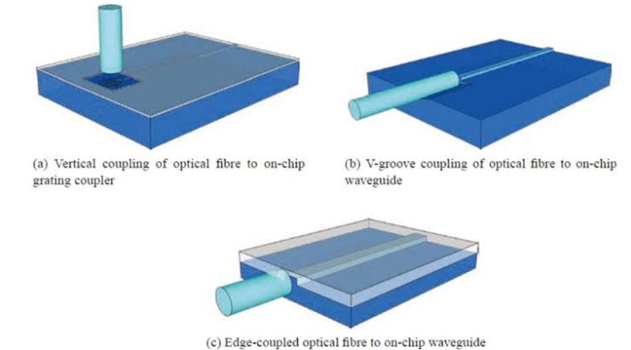
If CPO is to become a high-volume manufacturing technology, it needs an optical interface that can deliver low-loss coupling while also supporting pluggability, testing, and replacement.
These two papers are essentially answering that question. Paper 19 first establishes the fundamental process for attaching a glass coupler to a PIC. Paper 12 then connects this glass coupler to an expanded-beam connector, forming a more complete detachable edge-coupling CPO architecture.

Below we will share:
Review of Paper 19: V-groove and Glass Coupler Attachment Process
Materials and Epoxy Design
Passive Alignment Attachment Process and Dimensional Metrology
Process Optimization: Bonding Force and Epoxy Shrinkage
Review of Paper 12: Detachable Expanded-Beam Connector and Multi-scale Analysis
Why Expanded Beam Matters
Integrated Interpretation: From Process Unit to System Architecture

