High-Tolerance Optical I/O: Sumitomo Electric’s VCBEL Flip-Chip Integration on Glass
Original Articles By SemiVision Research (IEEE ECTC , Sumitomo )
At ECTC 2025, Sumitomo Electric Industries, Ltd. presented a groundbreaking paper titled “Flip-Chip Photonic-Electronic Integration Platform for Co-Packaged Optics using a Glass Substrate with Vertically-Coupled Beam Expanding Lens.” This work introduces an innovative CPO (Co-Packaged Optics) integration platform that combines a glass substrate with 3D-printed Vertically-Coupled Beam Expanding Lenses (VCBELs)—offering a novel solution to the long-standing alignment and packaging challenges in photonic-electronic co-integration.
According to the 2025 ECTC proceedings, a total of seven key papers were presented in the CPO domain. These contributions came from leading organizations including Intel, A*STAR and Rain Tree Photonics, Sumitomo Electric Industries, TSMC, Corning Research and Fraunhofer IZM, NVIDIA, and Furukawa Electric Co., Ltd.
The focus of today’s discussion is on Sumitomo’s concept paper, which stands out for its fusion of glass-based integration and additive micro-optics manufacturing, offering a glimpse into the next generation of scalable and high-density optical interconnect platforms.
Unlocking the Next Breakthrough in AI Photonic-Electronic Convergence
As artificial intelligence continues to scale in both training and inference workloads, traditional electrical interconnects are rapidly approaching their physical limits. Under the dual pressures of performance and energy efficiency, a critical innovation is quietly reshaping the foundational architecture of modern data centers—Co-Packaged Optics (CPO).
But the true challenge of CPO lies not only in chip-level integration. The core bottleneck is far more intricate: how can we achieve precise, stable optical alignment within standard packaging processes, especially under high-density integration requirements? This article explores a new generation of photonic-electronic integration platforms driven by glass substrates and Vertically-Coupled Beam Expanding Lenses (VCBELs)—revealing how this approach overcomes the tight ±0.1 μm optical alignment constraint and still operates reliably within the ±3 μm tolerance of conventional flip-chip assembly.
This isn’t just an advancement in packaging—it’s a photonic engine designed for the future of AI infrastructure.
Curious about how VCSELs can enable broadband optical coupling through glass waveguides? Wondering how laser-etched roughness challenges are being solved in practical integration?
In this piece, we uncover the complete packaging architecture, process flow, experimental results, and manufacturability outlook—offering a comprehensive look into one of the most viable CPO solutions on the horizon.
Unlock the full story to stay ahead in the coming wave of AI data center transformation.
Explosive Growth in Data Center Traffic × The Disruptive Opportunity of CPO
The rapid evolution of AI/ML models is driving unprecedented growth in data center traffic. According to McKinsey, global data center capacity is projected to grow at an annual rate of 19–33%, potentially doubling or even tripling by 2030. This exponential expansion signals a critical demand for interconnect technologies that are not only faster and lower in latency but also significantly more energy-efficient.
Traditional electronic interconnects are reaching the limits of their physical performance. In contrast, Co-Packaged Optics (CPO) offers a transformative solution by co-integrating photonic modules directly with electronic circuits. This tight integration dramatically increases bandwidth density while reducing overall power consumption—key to supporting next-generation AI infrastructure.
Yet, despite its promise, CPO is not easily brought into practice.
One of the core technical challenges lies in achieving precise optical alignment between photonic integrated circuits (PICs) and glass waveguides on a common glass substrate. While standard flip-chip bonding allows for ±3 μm placement accuracy—sufficient for electrical signaling—this is orders of magnitude too loose for optical connections, which typically require sub-micron alignment on the order of ±0.1 μm to avoid severe insertion loss.
Traditional solutions such as evanescent coupling offer better alignment tolerance but come with their own drawbacks. These include the need for long tapers and significant lateral space, which undermine the compactness and density requirements of modern CPO packaging. In short, they create a new bottleneck just as one is being solved.
For Paid Members, SemiVision will discuss topics on
Core Technology Innovation: VCBEL (Vertically‑Coupled Beam Expanding Lens)
Fabrication and Experimental Validation
Toward Scalable Production: From 3D Printing to Industrial Manufacturing
Co-Integration of EIC and PIC
Key Advantages of the Glass Substrate
System-Level Perspective and Future Outlook
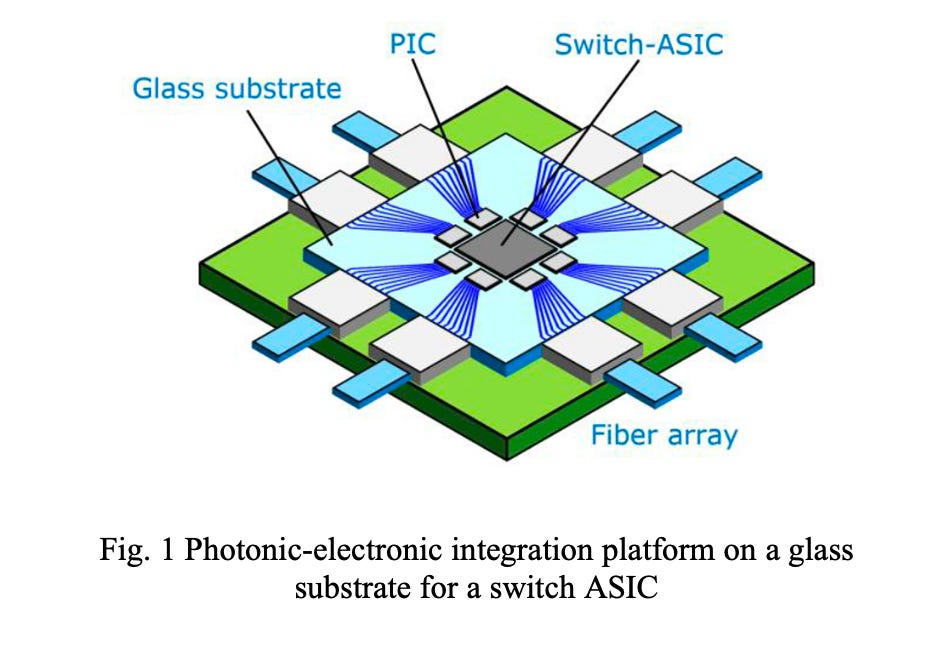
Photonic-electronic integration platform on a glass substrate for a switch ASIC
Cross-sectional view of the photonic-electronic integration glass substrate
Schematic image of the Vertically-Coupled Beam-Expanding Lens (VCBEL)
Optical switch module on a glass substrate
Simulated coupling efficiency vs. trench roughness height
Wavelength dependency of coupling efficiency with VCBELs
Alignment tolerance with VCBELs


