No InP, No Optical Transceiver ?!
Original Article By SemiVision Research [Reading time: 7 mins]

No InP, No Optical Transceiver ?!

The artificial-intelligence infrastructure boom is creating a new semiconductor bottleneck, but it is not located inside the GPU.
It is located inside the optical link.
As AI clusters expand from thousands to hundreds of thousands of accelerators, data must move rapidly between GPUs, switches, racks and eventually entire data-center campuses. Copper connections are increasingly constrained by reach, signal integrity and power consumption. Optical interconnects are therefore moving closer to the processor, from conventional pluggable transceivers toward near-packaged optics and co-packaged optics.
Yet every optical network requires a source of light. Silicon can route, split and modulate light, but conventional silicon is an inefficient light emitter because of its indirect bandgap. Direct-bandgap III-V materials, especially indium phosphide, remain the commercially established solution for generating and detecting light at the wavelengths used in high-speed data-center communications.
Strictly speaking, “No InP, no optical transceiver” is an industry shorthand rather than a universal scientific rule. Some short-reach multimode transceivers use gallium-arsenide VCSELs.
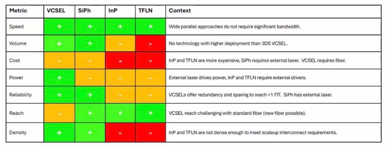
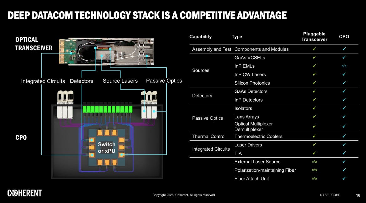
But for the high-speed single-mode links increasingly used in 800G, 1.6T and future 3.2T systems, InP-based EMLs, continuous-wave lasers and photodetectors have become foundational components. Coherent’s current product roadmap, for example, combines InP EMLs for pluggable modules, high-power InP CW lasers for silicon-photonics transceivers and CPO, and InP photodiodes for receiving optical signals.
Below we will share:
Where InP Capacity Is Expanding
Supply-Chain Outlook