

Sailing into the AI Supercomputing Era: Key Technologies and Industry Trends at OCP APAC 2025
Original Article By SemiVision Research (OCP,Hotchip,ECTC,Broadcom,Nvidia,AMD , Marvell ,TSMC,Nvidia,OpenAI,NTT,Meta,Google,Microsoft,ASE ,Astera Labs,ARM, MTK,Coherent,iPronics,TE,Oriole Networks)

At a time when large language models are moving beyond the “parameter arms race,” the launch of GPT-5 has shifted the industry’s focus from “can it be done” to “is it usable, affordable, and widely applicable.” OpenAI’s key contribution lies in narrowing the gap between models and real-world workflows through engineering and product methodology. On one hand, it has chosen a favorable balance in the price–performance–reliability triangle, lowering inference costs, stabilizing long-context performance, and reducing hallucination rates—thus improving the success rate and consistency of everyday tasks such as office work, productivity, content creation, analysis, and software development.
On the other hand, it has provided developers with a more complete toolchain and runtime (spanning function calling, file/retrieval, rules and memory management, multimodal input/output, and stronger programmatic reasoning), reducing the friction of going from demo to deployment to a predictable level.
The result is that AI has transformed from “demonstrable features” into “deliverable products,” from point-level automation into auditable, governable, ROI-measurable workflow components—driving enterprises to embed model capabilities into sales, customer support, compliance, R&D, supply chains, and data governance.
At the same time, OpenAI is leveraging both product and distribution to convert model advantages into retention and revenue. For end users, ChatGPT serves as a “high-frequency entry point” for long-form writing, meeting notes, summarization, image interpretation, and lightweight coding assistance—aligning closely with users’ time and workflow needs.
For enterprises and developers, APIs and enterprise-grade features (permissions/auditing, data isolation, privatization, compliance options) make embedding models into existing systems more controllable, while smoothly integrating with DevOps, MLOps, and data stack toolchains. More importantly, OpenAI continues to abstract “model capabilities” into “composable abilities”: lightweight agents composed of task rules, tool use, memory, and retrieval. These can be easily deployed in CRM, knowledge bases, ticketing, and internal process automation. This “semi-automated with human oversight” form balances compliance and efficiency and diffuses more easily within large organizations. From a commercialization perspective, the pathway is clear and repeatable: high-frequency entry points drive stickiness and feedback, APIs expand the boundary, and enterprise features secure budgets and decision-making—together forming a reinforcing feedback loop.
The global application ecosystem is also maturing. On the user side, stable subscription and payment structures have emerged across writing, design, video, translation, data analysis, and programming assistance. On the enterprise side, the most resilient demand does not come from flashy features but from embedding AI into “processes with clear KPIs”—shortening support ticket resolution time, improving sales conversion, reducing R&D defect rates, or increasing efficiency in financial report review and compliance. Once the foundational model is strong enough and its cost/quality predictable, the determinant of unit economics shifts from “model benchmarks” to “scenario fit and distribution efficiency.” Whoever is closest to OS-level entry points, collaboration platforms, or content distribution hubs is best positioned to monetize compute into cash flow. This explains why the U.S. market is faster in productization: software distribution, cloud infrastructure, compliance systems, and procurement workflows are mature, lowering friction from pilot to scale. OpenAI provides the lowest-friction building blocks along this chain.
In China, due to regulatory, data boundary, and infrastructure differences, local vendors tend to focus on industry project delivery and system integration—embedding models into existing workflows. The broader lesson for global players is the same: sustainable value does not come from one-off model benchmarks, but from long-term integration into enterprise data assets and governance frameworks, producing repeatable templates through reliable delivery. In other words, regardless of market differences, sustainable AI growth comes from turning “models into components, components into workflows, and workflows into revenue.” For U.S. readers and decision-makers, the point is not short-term metrics but who can establish clear engineering and compliance paths for data governance, workflow orchestration, permissions/auditing, and hybrid cloud/on-prem deployment. OpenAI’s leadership in productization and developer ecosystems is accelerating the shift from concept to scaled reality.
In sum, the significance of GPT-5 is not in declaring a paradigm shift but in creating a pragmatic engineering curve that links usability, affordability, and scalability into a commercial trajectory. Lower costs, better stability, more complete development/runtime capabilities, and dual push across consumer and enterprise use cases make up OpenAI’s engine for AI adoption. For enterprises and developers, the priority is no longer chasing extreme benchmarks, but embedding models into critical workflows with governance, auditing, and measurable ROI. For investors and industry observers, the next stage of defensibility lies in integrating entry points, data, and workflows into reusable, productized capabilities—where OpenAI is turning abstract intelligence into concrete business outcomes.
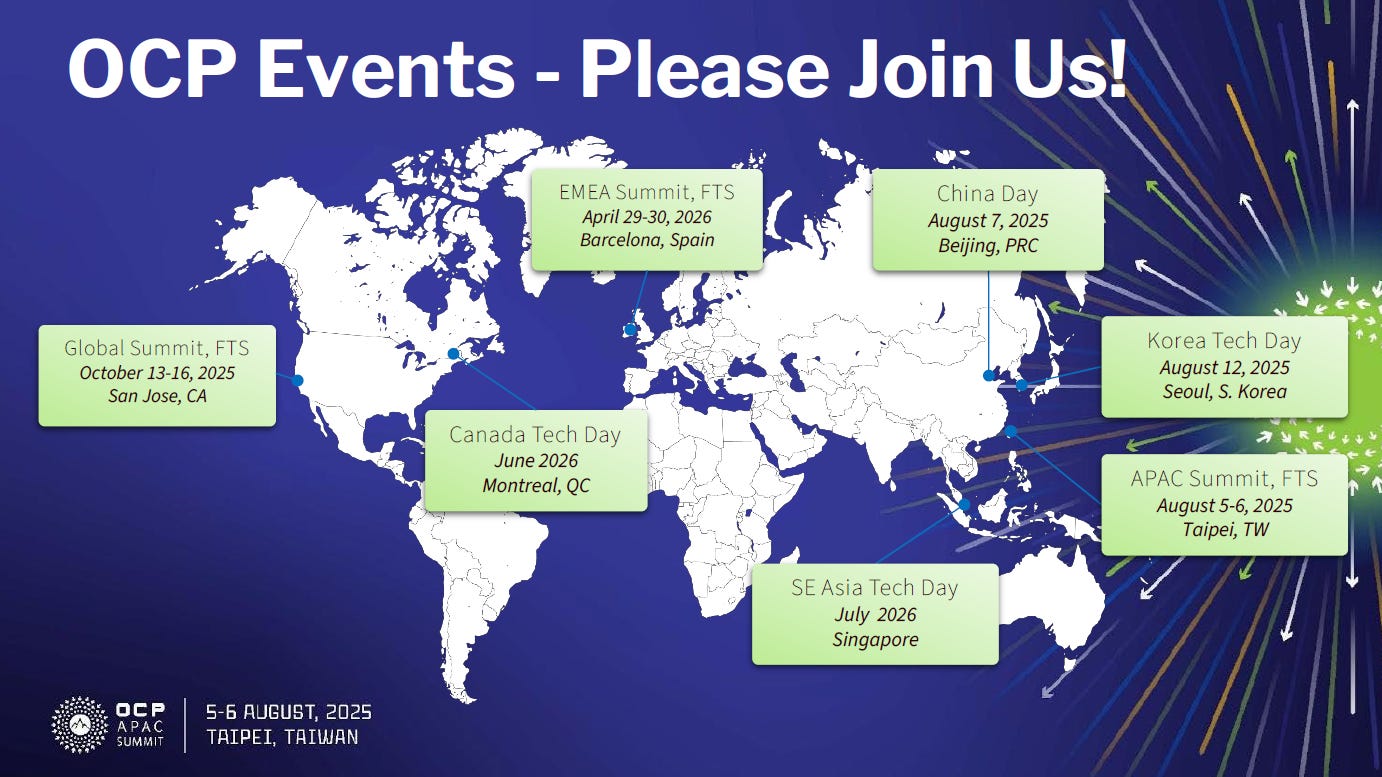
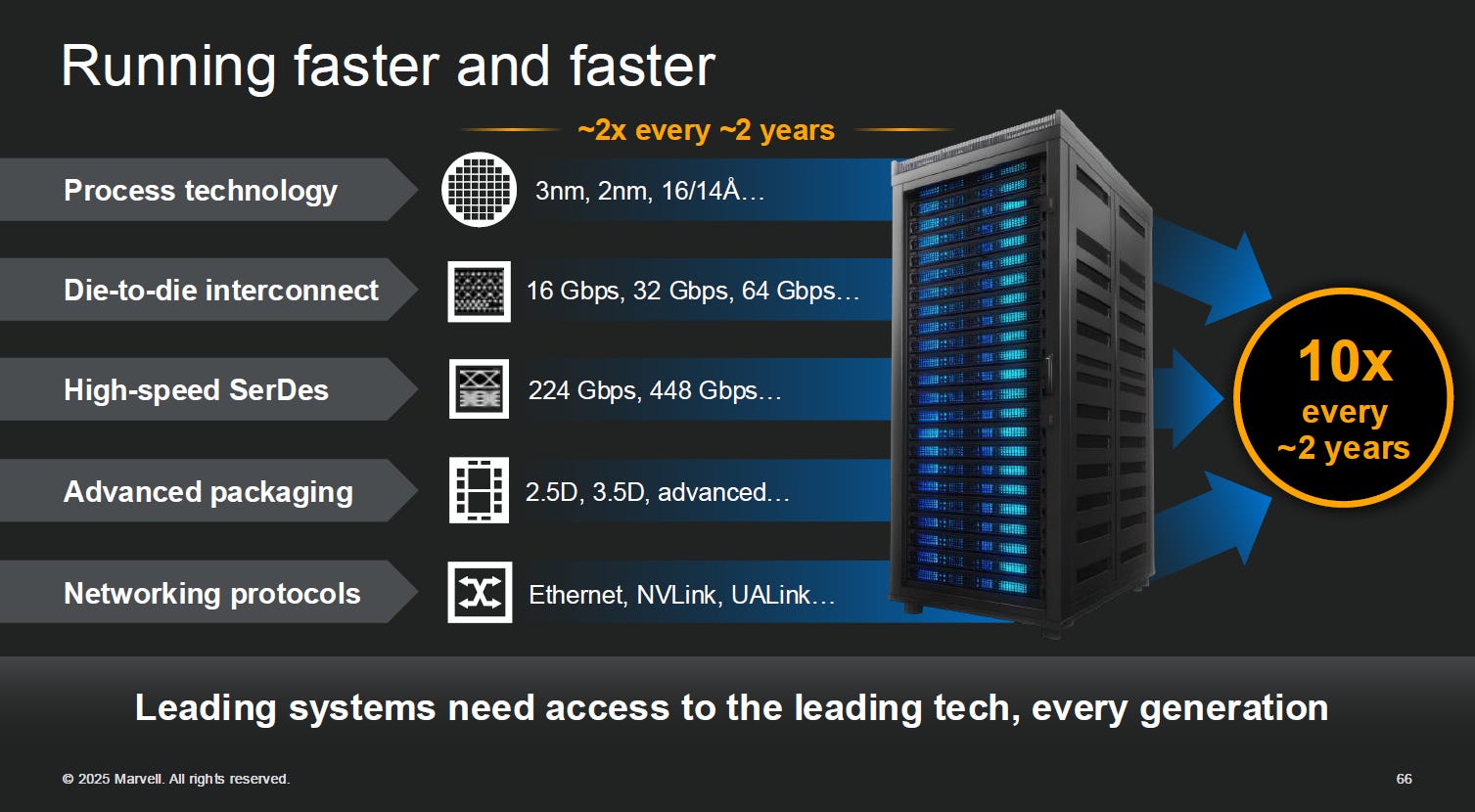
As GPT-5 shifts the industry’s focus toward usability, affordability, and scalability, what truly needs upgrading is the physical infrastructure that carries these workflows—racks, power, cooling, networking, and sustainability. OpenAI’s product/engineering abstractions—turning models into modular capabilities embedded into governable, auditable workflows—translate on the cloud side into new workload profiles: longer contexts, higher concurrency, tighter latency/throughput coordination, and volatile cost elasticity. These constraints cannot be solved by one vendor in isolation; they are digested and standardized in the open collaboration arenas led by CSPs. This is precisely the role of the Open Compute Project (OCP)—a pipeline that translates “model requirements” into “hardware specifications and operational conditions.” At OCP, hyperscalers like Meta, Google, Microsoft, and AWS align on cabinet power, liquid cooling, networking/acceleration, and circular storage economy through open specs and reference designs, turning hardware/software, supply chains, and operations into a common language. In 2025, OCP’s summit cadence is clear: the OCP APAC Summit in Taipei (Aug 5) and the OCP Global Summit in San Jose (Oct 13–16), the largest annual gathering for open compute, focused on pushing next-gen datacenter design toward deployable consensus.

In the AI era, several key shifts are visible along this “workflow-to-datacenter translation chain.” First, a “photonics-first” networking view: as applications move toward long-context multi-agent coordination, trade-offs across CXL/PCIe domain architectures and Ethernet/InfiniBand must balance power, latency, and maintainability. OCP’s recent educational activities on Co-Packaged Optics (CPO) reliability reflect the effort to shrink the gap between technical feasibility and scale feasibility by integrating modules, cooling, power, and testing into unified design units. Second, liquid cooling as mainstream grammar: from rack-level to campus-level cooling, standard interfaces, maintenance flows, and safety compliance need community-driven definition, or TCO and safety will fragment. Third, sustainability as a native feature: from green concrete to disk recycling and carbon label standardization, OCP embeds ESG into hardware lifecycles, making procurement, deployment, and recycling auditable. These three strands converge at OCP’s conferences, working groups, and contribution databases into replicable industrial rhythms: open specs → reference designs → testing methods → supply chain recipes.
Viewed this way, OpenAI is operationalizing the growth engine of “model capability → productization → workflows,” while OCP flattens the supply curve of “racks → datacenters → campuses.” The former defines the demand function for compute and software applications; the latter decomposes that demand into standardized, auditable, deployable industrial components. The implications for participants are concrete: software/application teams should translate SLA and latency/concurrency models into explicit networking/cooling targets aligned with OCP standards; component, system, and materials suppliers should time product definitions and roadmaps to OCP events (absorbing local CSP needs at APAC, aligning with global standards at the Global Summit); operations and ESG teams should embed sustainability and recycling into early procurement/design stages. From this vantage point, AI “scalable deployment” is no longer a vendor’s point solution but a chainwide collaboration model: workflows defined by OpenAI, translated into deployable standards via CSP–OCP coordination. For U.S. readers and decision-makers, the strategy is clear: align product and roadmap with OCP’s cadence and language, trading lower friction for faster deployment and stronger unit economics in the next wave of AI commercialization.
(Note: OCP APAC Summit will be held Aug 5, 2025, in Taipei; OCP Global Summit will take place Oct 13–16, 2025, at the San Jose Convention Center.)
The 2025 APAC OCP event has concluded, marking another highly rewarding and important forum. SemiVision has summarized some key takeaways from this year’s forum. The OCP Forum stands out as an innovative, cross-disciplinary platform, and serves as an excellent opportunity for professionals in the semiconductor industry to recharge their technical knowledge. Next on the calendar is Hot Chips, which is another highly significant event.

First, we observed that OCP’s scope has expanded beyond racks, now covering AI chips, CoWoS, and CPO technologies.
At the same time, NTT Device shared extensive insights into silicon photonics technology, while the IWON Forum explored the concept of an All-Optics Network. We also noted active discussions around OCS, with OCP now including it as a planned project.
In previous articles, we have covered numerous forums and papers from ECTC. The call for papers for ECTC 2026 will open soon. Looking ahead, the major events for 2025 will be Hot Chips, Semicon Taiwan, IEDM, and ECOC.
Hot Chips 2025
Website: https://hotchips.org/
Hot Chips 2025 will be held Sunday, August 24 - Tuesday, August 26, 2025 at Memorial Auditorium, Stanford, Palo Alto, CA.
The 2026 IEEE Electronic Components and Technology Conference (ECTC), the premier technical conference and product exhibition for the world’s semiconductor packaging industry, has announced a Call for Papers. ECTC 2026 will take place May 26-29, 2026 at the JW Marriott & Ritz-Carlton Grande Lakes Resort in Orlando, FL. More than 2,000 scientists, engineers and business people from more than 20 countries are expected to attend.
Abstract submission will open on August 18, 2025 and the deadline for submissions is October 6, 2025. For all details and to submit an abstract, please visit the ECTC 2026 Call for Papers.
The ECTC 2026 technical program will address new developments, trends and applications for a broad range of topics, including components, materials, assembly, reliability, modeling, interconnect design and technology, device and system packaging, heterogeneous integration, chiplet architectures, hybrid bonding, WLP and PLP, fan-out and fan-in packaging, flip-chip technologies, integrated photonics and optoelectronics, LEDs, 5G, quantum computing and systems, and other emerging technologies in electronics packaging.
Applied Reliability
Assembly and Manufacturing Technology
Electrical Design and Analysis
Emerging Technologies
Interconnections
RF, High-Speed Components & Systems
Materials & Processing
Thermal/Mechanical Simulation & Characterization
Packaging Technologies
Photonics
Interactive Presentations
At the recently concluded 2025 APAC OCP Taiwan event, what unfolded was far more than a forum on “open compute”—it was a declaration of a full-stack industry transformation, spanning from racks to silicon, from fiber optics to firmware. This high-density, cross-disciplinary exchange placed AI/HPC computing topologies, optoelectronic packaging, interconnect protocols, thermal and power systems, and supply chain strategies onto the same strategic blueprint.
This was not a mere product showcase, but a deep alignment exercise among engineers, supply chain decision-makers, and system architects. Core players including Broadcom, TSMC, ASE, Meta, Astera Labs, the UALink Consortium, and NTT revealed critical design trade-offs for the next generation of computing infrastructure—ranging from Scale-up versus Scale-out topology choices, to CPO and CoWoS efficiency boundaries, to deployable OCS and all-optical network solutions. More significantly, Taiwan, South Korea, and mainland China will no longer be isolated markets, but interconnected hubs within an Asia-Pacific “silicon ecosystem” — each contributing unique strengths in manufacturing density, memory modularization, and all-optical system integration.
If you want to know—
Why has OCP’s scope expanded from rack specifications to the entire silicon ecosystem?
What packaging and testing hurdles must CPO overcome to move from concept to mass production?
How Broadcom, AMD, and NVIDIA’s Scale-up and Scale-out strategies are shaping the AI factory landscape?
Whether OCS and all-optical networks will become the true inflection point for million-GPU clusters?
How Taiwan can seize a “Golden Decade” amid the supply chain tug-of-war between de-globalization and re-globalization?
This in-depth analysis takes you behind the scenes of the forum, decoding the engineering logic and industrial positioning that will define the computing landscape for the next decade. Understand this, and you’ll understand the hidden cards in the next AI infrastructure race.
In addition, when we think of Broadcom, another company that comes to mind is Marvell.
OCP (Open Compute Project) Global Summit – Marvell’s Showcase and Presentations
The OCP Global Summit is a major event for the open hardware community, held every fall in San Jose, California. Marvell frequently uses this platform to showcase its next-generation data infrastructure chips and optical modules, while also sharing its technical directions through various talks.
2024 OCP Global Summit
Exhibit and Demonstrations:
The event took place on October 15–17, 2024 at the San Jose Convention Center. Marvell exhibited at booth B1, featuring products such as the 1.6 Tb/s PAM4 DSP, Gen6 PCIe retimers, COLORZ® 800 ZR/ZR+ coherent modules, Orion coherent DSP, Spica and Nova PAM4 DSPs, and the Teralynx® Ethernet switch family.
Talks and Panels:
Marvell arranged multiple speaking sessions:
On October 15, the keynote panel “Scaling AI Clusters: Interconnects and Memory” featured Nigel Alvares, VP of Strategy.
Khurram Malik discussed the challenges and opportunities of Structera CXL memory devices; Venu Balasubramonian explored AI and cloud DSPs at the expo floor; Nick Kucharewski moderated the Open Networking Switches breakout.
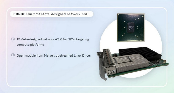
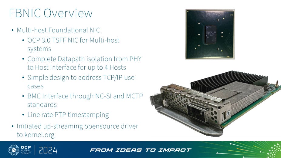
On October 16, several panels included: Jack Harwood joining the AI/HPC Future Connectivity session to discuss the role of CXL and PCIe in AI networking; Dr. Loi Nguyen participating in an industry panel on the right path to AI interconnects; Meta’s Dave Fenton presenting FBNIC – Meta’s control plane; plus a multi-vendor AI systems panel.
On October 17, Marvell researchers presented topics such as using CXL for near-memory accelerators to overcome the memory wall.

Marvell’s SerDes Optical Engines and Design Services


3D SiPho Optical Engine and Photonic Packaging
3D SiPho Optical Engine: At OFC 2024, Marvell showcased the industry’s first 3D Silicon Photonics (3D SiPho) engine integrating 32 × 200 Gb/s electrical/optical channels into a single device. Using 3D packaging, the engine combines hundreds of components—waveguides, modulators, photodetectors, modulator drivers, transimpedance amplifiers, microcontrollers, and other passive devices—into a unified package. It delivers 2× bandwidth, 2× I/O density, and ~30% lower power consumption compared to 100G-class electro-optical solutions. The 3D SiPho optical engine can be deployed in pluggable modules or future co-packaged optics (CPO), addressing AI datacenters’ demand for high-bandwidth, low-power optical interconnects.
Co-Packaged Optics (CPO) Architecture: In January 2025, Marvell announced its CPO architecture, which places the 3D SiPho optical engine alongside customers’ AI accelerators (XPUs), HBM chips, and other components on the same substrate. By integrating optics directly within the XPU package via high-speed SerDes and die-to-die interfaces, the design eliminates long-reach electrical traces, boosting XPU-to-XPU link rate and distance by up to 100× versus cables, while reducing latency and power. Combined with Marvell’s 6.4 Tb/s 3D SiPho engine, the CPO architecture delivers 32 × 200 Gb/s electro-optical channels in a single device, enabling high-speed optical interconnects for large-scale AI servers.
SerDes IP and Optical Engine Design Services
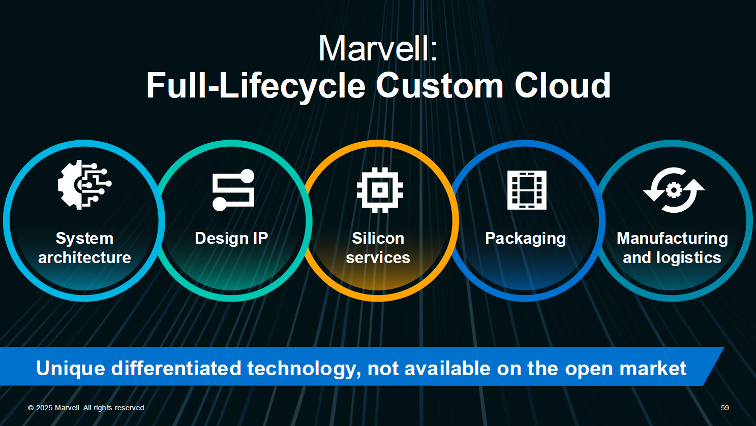
Marvell’s custom ASIC platform provides a rich IP portfolio and design services for building cloud and AI infrastructure chips:
High-Speed SerDes and Interconnect IP: At 3nm, Marvell offers IP blocks such as 112G XSR SerDes, long-reach SerDes, PCIe Gen6/CXL 3.0 SerDes, and 240 Tb/s parallel die-to-die interconnects. These IPs support all packaging options and are deployed in Teralynx® switches, PAM4 and coherent DSPs, Alaska® Ethernet PHYs, OCTEON® processors, Bravera™ storage controllers, and custom ASICs.
SerDes Optical Engine Design Services: Marvell’s IP portfolio includes 112G XSR and 224G SerDes, PCIe Gen6/CXL 3.0 SerDes, 240 Tb/s die-to-die interconnects, ARM SoC subsystems, and low-cost packaging options. These enable performance, power, and area optimization for customer ASICs. Its mixed-signal SerDes IP supports 1 Gbps to >112 Gbps, covering Ethernet, PCIe, SAS, SATA, and more. Combined with 3D SiPho engines, these IPs can power pluggable modules, co-packaged optics, and chiplet interconnects.
UALink Scale-Up Solution: In June 2025, Marvell introduced its proprietary UALink scale-up solution, integrating 224 Gb/s SerDes, UALink PHY IP, configurable controller IP, scalable low-latency switch fabrics, and packaging options supporting both co-packaged copper and optics. This enables low-latency, scalable interconnects across hundreds to thousands of AI accelerators, complementing Marvell’s custom silicon to build high-performance AI clusters.
3. Collaboration with AWS
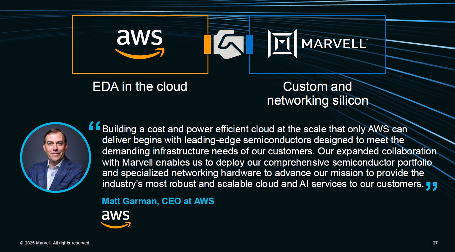
In December 2024, Marvell announced an expanded strategic partnership with Amazon Web Services (AWS):
Supply Scope: Over the next five years, Marvell will provide AWS with a broad range of datacenter semiconductors, including custom AI silicon, optical DSPs, active cable (AEC) DSPs, PCIe retimers, datacenter optical modules, and Ethernet switch chips.
Cloud Design Services: AWS will provide cloud-based EDA infrastructure to Marvell, enabling large-scale parallelization of silicon design workloads on AWS, shortening design cycles, and dynamically scaling compute resources.
Executive Perspectives: Marvell CEO Matt Murphy noted that AWS’s EDA infrastructure provides Marvell with dynamic design scalability. AWS CEO Matt Garman stated that Marvell’s semiconductor technologies will enhance the efficiency of AWS’s cloud and AI services, lowering TCO and accelerating time-to-market. This partnership strengthens AWS’s deployment of advanced networking and storage solutions while giving Marvell greater design flexibility.
Marvell at the OCP Global Summit
Since 2022, Marvell has actively participated in the OCP Global Summit at the San Jose Convention Center, presenting its cloud and AI infrastructure portfolio. The company has highlighted 1.6T PAM4 DSPs, CXL memory devices, co-packaged optics, and switching/optical modules, collaborating with partners like Arm and Microsoft to demonstrate interconnect and optoelectronic conversion technologies. The 2025 OCP Global Summit, themed “Leading the Future of AI”, will again take place in San Jose.
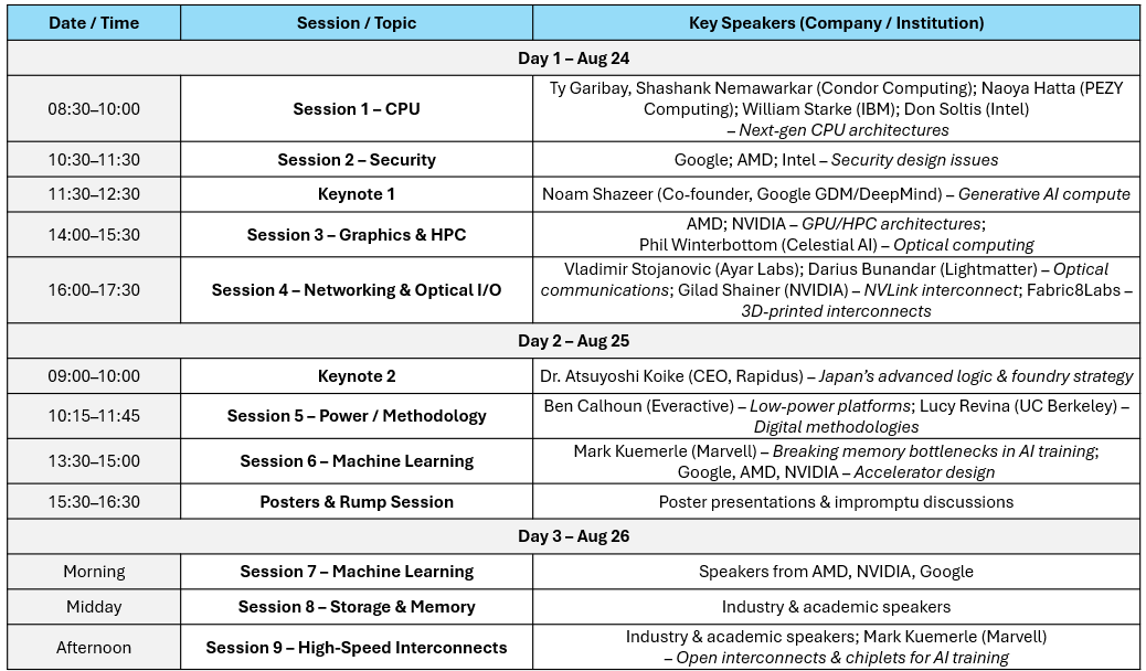
Hot Chips 2025 Keynote Speaker
At HC37 (Hot Chips 2025), which focuses on CPUs, optical communications, machine learning, and security, Marvell’s Mark Kuemerle will join thought leaders such as Google DeepMind co-founder Noam Shazeer and Rapidus CEO Dr. Atsuyoshi Koike to present the future of AI hardware and interconnect innovation.
Marvell is aggressively leveraging its high-speed SerDes, 3D SiPho optical engines, and custom design services to advance innovation in cloud and AI datacenters. Through collaborations with AWS and contributions to the OCP community, Marvell is accelerating the growth of the open hardware ecosystem and driving the next wave of AI-scale infrastructure.
For Paid Members , SemiVision will discuss topics on
OCP’s Shift from “Racks” to the “Silicon Ecosystem”
Broadcom : Dual-Engine Compute Architecture: The Engineering Logic of Scale-up and Scale-out
AMD : Open Standards and Interoperability: Dual-Track Strategy of UALink × UEC
Broadcom’s Ethernet Approach: Tomahawk Ultra and AI Fabric Router
Advanced Packaging × Optoelectronic Integration: TSMC’s CoWoS + COUPE
OSAT and Modularization: ASE’s Panel and CoPoS Strategy
OCS and All-Optical Networks: From Data Center Cabling to Campus-Orchestration
NTT IOWN and the All-Optical Network
China’s dOCS and Supernode Solutions
Astera Labs:Interconnect, Memory, and Storage: PCIe Gen6, CXL3, and Gearbox
Key Factors to Watch in Semiconductor Technology