Unlocking the Future: TSMC’s Bold Strategy for the 2nm Revolution!
Original Articles by SemiVision Research

Before reading this article ,you can refer to previous articles
AI Joins the 3nm Battle: TSMC Receives a Surge of Orders!
TSMC N3 and N2 Nodes: Shaping the Next Era of Chip Manufacturing
TSMC's N2 and the Power of PPACt: Driving the Future of Semiconductor Innovation
TSMC’s Mother Fab: The Heart of Advanced Process Development
Can SMIC Overcome Its Bottleneck Solely Through DUV Immersion? SMIC vs TSMC?
TSMC's 2nm Process: The Next Leap in Semiconductor Innovation
TSMC is currently advancing its 2-nanometer (2nm) process technology, a development poised to mark a significant milestone in global semiconductor innovation. As the world’s leading pure-play foundry, TSMC’s move into 2nm underscores not only its technological prowess but also its strategic importance in the global supply chain.
TSMC’s 2nm Expansion Progress: Government and Industry Collaboration in Focus

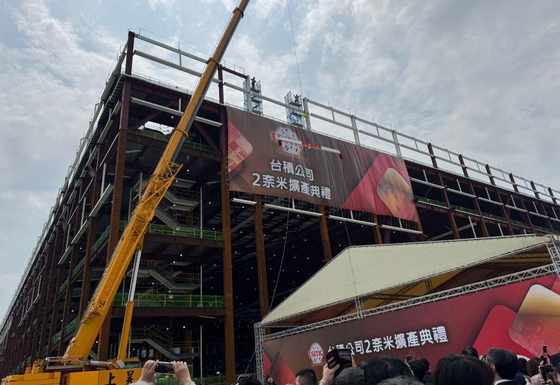
On March 31, 2025, TSMC held an expansion ceremony for its 2nm production facility in Kaohsiung, marking a significant milestone in Taiwan’s semiconductor advanced manufacturing expansion. The event was hosted by TSMC’s Executive Vice President and Co-Chief Operating Officer, Y.P. Chin, with the presence of government officials such as Premier Cho Jung-tai and Kaohsiung Mayor Chen Chi-mai, alongside TSMC’s supply chain partners, witnessing this remarkable achievement.

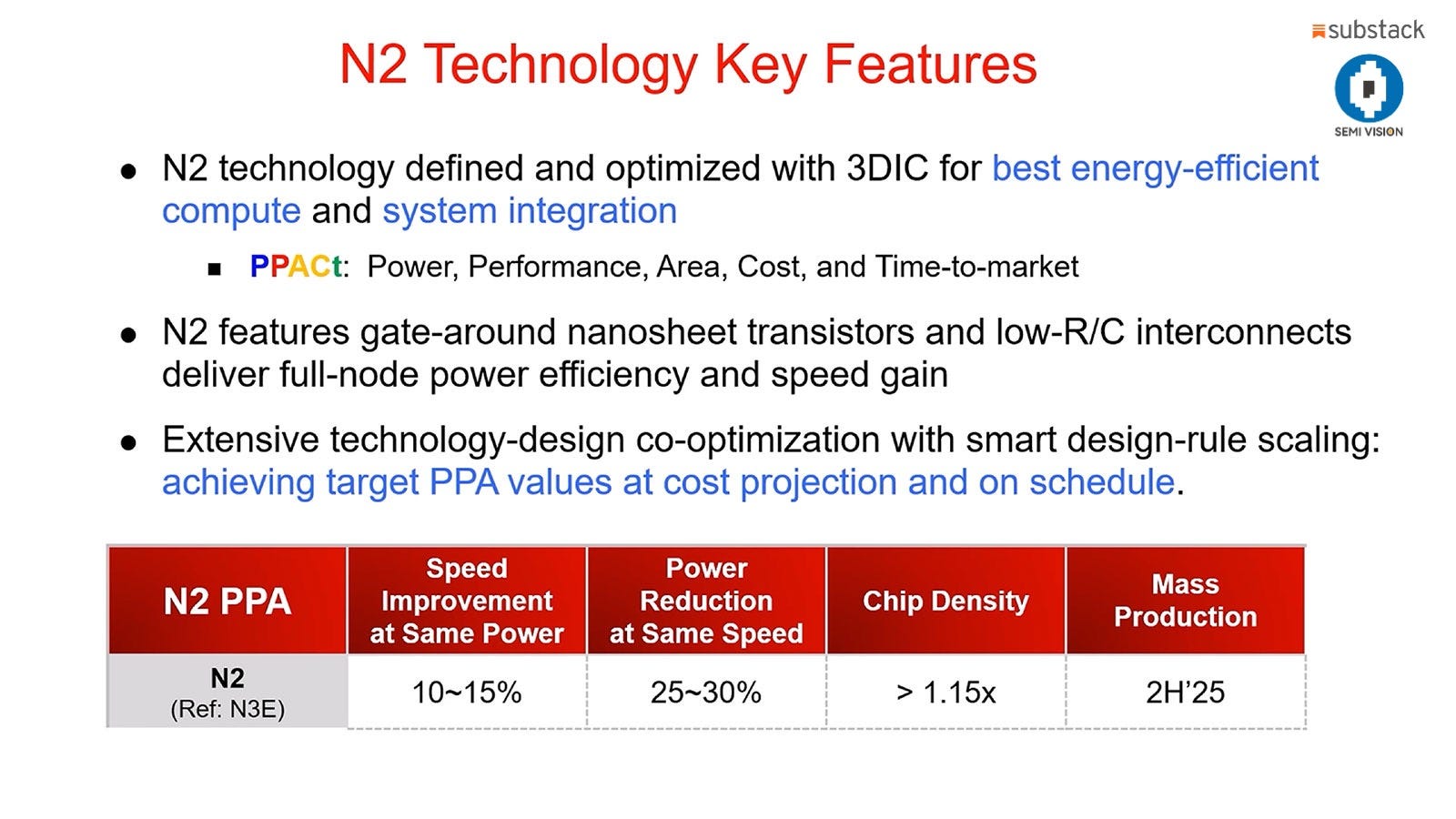
Y.P. Chin stated that TSMC’s 2nm process technology is expected to enter mass production as scheduled in the second half of 2025 and will be widely used in supercomputers, mobile devices, cloud data centers, and other cutting-edge technology applications. Compared to the 3nm process, the 2nm process offers a 10% to 15% speed improvement at the same power level or a 25% to 30% power reduction at the same speed.

During the ceremony, Premier Cho Jung-tai expressed his gratitude to TSMC for maintaining its “Global Deployment, Rooted in Taiwan” strategy, reaffirming the government’s commitment to supporting domestic companies in strengthening cooperation and ensuring that Taiwan remains a critical hub for global manufacturing and economic growth.
Additionally, TSMC’s Wafer Fab 22 in Kaohsiung represents an investment of over NT$1.5 trillion and is expected to create over 7,000 high-tech job opportunities and more than 20,000 construction-related jobs. These investments will further drive industrial development and boost the local economy.
In summary, TSMC’s 2nm process development is progressing smoothly, and its continuous expansion in Kaohsiung underscores its commitment to advancing next-generation process technologies while strengthening Taiwan’s position as a global semiconductor manufacturing hub.
Recent Developments on TSMC’s 2nm Process:
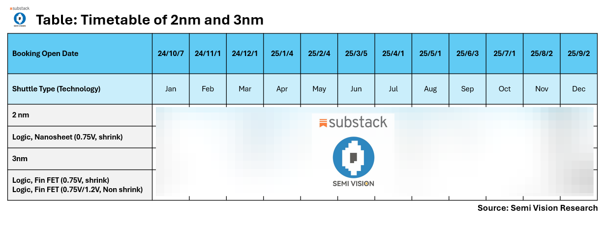
Accepting 2nm Wafer Orders
TSMC is reportedly set to start accepting orders for its 2nm wafers on April 1, 2025. Apple is expected to be among the first customers, potentially using the N2 technology in its A20 chips for the iPhone 18 series, launching in 2026.,based on insights from SemiVision Research, Apple is likely to adopt the 2nm process for its high-end smartphones, as the technology remains highly complex and costly. Currently, a single 2nm wafer is estimated to cost around OOOOO dollars.
2nm Process Technology Progress
TSMC’s N2 node is progressing steadily and will feature its first-generation nanosheet transistor architecture, promising improvements in performance and power efficiency across all platform variants. The company expects volume production to begin in 2H 2025.
The next generation following TSMC’s N2 process is A16, which can be seen as offering improved power consumption performance. At the same time, NVIDIA is actively considering both TSMC Arizona and Intel’s 18A as key “Made in USA” manufacturing platforms. This could lead to a shift in production capacity, aligning with the Trump administration’s push for “AI chips made in the USA” and the broader slogan of “Make America Great Again.”
Nvidia is actively shifting part of its production to TSMC Arizona and Intel 18A. According to a survey by SemiVision Research, the proportion of Nvidia’s chip production in Taiwan and the United States is expected to reach O:O by 2028.
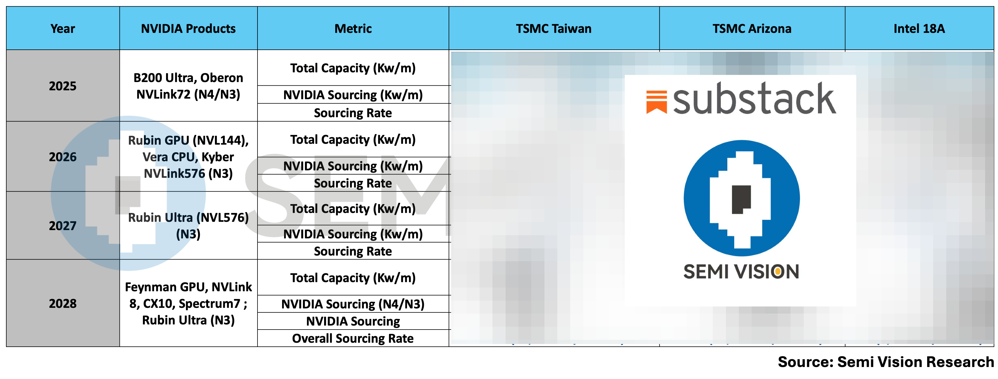
At the same time, in response to the push for U.S. manufacturing, TSMC has planned advanced process nodes in both Taiwan and the United States. However, TSMC’s technological strategy in the United States can be described as a dual-track approach.
Capacity Expansion Plans
TSMC is expanding its 2nm manufacturing facilities in Baoshan (Hsinchu) and Kaohsiung, aiming for a monthly capacity of OOOOO wafers by the end of 2025, with potential scaling up to OOOOO wafers per month. A ceremony marking the capacity expansion at the Kaohsiung fab is scheduled for March 31, signaling the move toward mass production.
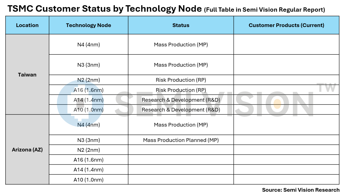
According to SemiVision Research, the current status of TSMC’s main N4/N3/N2 nodes is as follows:

Yield and Production Readiness
Reports indicate that the trial production yield for TSMC’s 2nm process has reached OO%, signaling readiness for commercial-scale manufacturing. A significant number of customers are expected to line up for early access to production capacity.
Competitive Landscape
TSMC faces growing competition from Samsung and Intel, both of which are also developing 2nm technologies. Samsung aims to start mass production in 2025, while Intel 2 nm (18A) targets 2025. This underscores the intense race in the advanced process node sector.


Intel Showcases Groundbreaking Innovations at IEDM 2024
The Ever-Shifting Relationship Between TSMC and Intel: A History of Competition and Cooperation
SemiVison: TSMC and Intel JV possible?
Captain Intel: Reassembling the Semiconductor Avengers
Intel’s Secret Weapon: The 18A Process and Its Bold Comeback
For Paid Members , SemiVison Research will discuss following topics on
TSMC N2 Fab Location(Mapping)
Unlocking the Invisible: The Art of Semiconductor Fabrication
Key Milestones and Timeline
Technical Innovations to GAA FinFET
N2 Innovation : Architectural Shift FinFET to GAA and A16 with BSPDN
PPAc Roadmap for logic device
Key Customers and Adoption in N2
N2 Production Sites (Oversea Foundry and Taiwan Location)
Challenges Ahead in N2 Process
From FinFET to GAA: The Rising Complexity of Transistor Inspection(KLA, Rigaku, and the Evolving Landscape of Semiconductor Metrology in the GAA Era)
Navigating Complexity with Innovation
TSMC N2 Highlight
TSMC IEDM 2nm Paper Highlight