


A*STAR — Powering the Future of Silicon Photonics and Advanced Packaging
Original Article by SemiVision Research ( IEEE ECTC , A*STAR , Rain Tree Photonic)


This SemiVision article aims to explore the key themes of CPO (Co-Packaged Optics) discussed at IEEE ECTC 2025, with a focus on a standout paper contributed by A*STAR, a world-class research institution known for its prolific and high-impact publications.
ECTC is one of the most prestigious and technically rich conferences in the semiconductor industry.
It brings together a wide spectrum of participants, including leading global corporations and top-tier research institutions, all actively contributing to the advancement of packaging, interconnect, and system integration technologies. Each year, ECTC serves as a platform for unveiling cutting-edge innovations, fostering collaboration across industry and academia, and setting the direction for the future of advanced semiconductor technologies.


The paper provides detailed insights into the optical engine’s design, key features, and simulation/testing results related to high-frequency electrical performance, thermo-mechanical stress, and thermal dissipation, demonstrating its advantages in supporting high-speed data transmission and meeting the demanding requirements of data centers.
The packaging approach in this paper employs Fan-Out Wafer-Level Packaging (FOWLP) while incorporating the concept of a glass interposer. While companies like Broadcom have already showcased the potential of FOWLP in silicon photonics packaging, A*STAR’s work introduces a novel angle by integrating glass, prompting deeper exploration into the role of glass in CPO architectures.
At ECTC 2025, numerous papers delve into the use of glass materials in advanced packaging—many of them from major industry players and material suppliers—highlighting a strong industry trend worth close attention.

IME Singapore: A Key R&D Hub for Silicon Photonics and Advanced Packaging in Asia
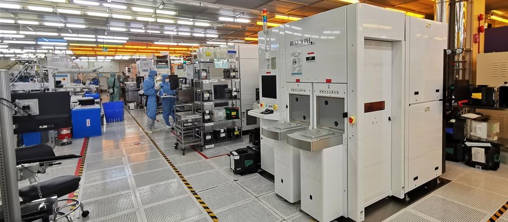
The Institute of Microelectronics (IME) in Singapore has emerged as a strategic research and development hub in Asia, specializing in silicon photonics and advanced packaging technologies. Positioned at the intersection of semiconductor innovation and industrial collaboration, IME plays a vital role in driving next-generation solutions for AI, data centers, and heterogeneous integration.

With strong government support and close partnerships with global industry leaders, IME is not only pushing the frontiers of co-packaged optics (CPO), fan-out packaging (FOWLP), and glass interposer technologies, but also helping to shape the broader ecosystem for chiplet integration, high-speed interconnects, and energy-efficient data transmission.
As Asia’s demand for scalable, high-performance semiconductor solutions grows, IME is solidifying its status as a go-to innovation engine—connecting materials research, process engineering, and system-level design in a comprehensive platform that fuels the future of electronics.
IME: Singapore’s National-Level Technology Incubator for Semiconductors
Founded in 1991, the Institute of Microelectronics (IME) operates under A*STAR (Agency for Science, Technology and Research) with the mission of advancing microelectronics research to help Singapore build a complete semiconductor value chain—from materials and chips to modules and systems. IME is more than just a research institute; it serves as a technology translation and industrialization platform, delivering forward-looking solutions for global partners.
Six Core Technology Focus Areas

Advanced Packaging & Heterogeneous Integration
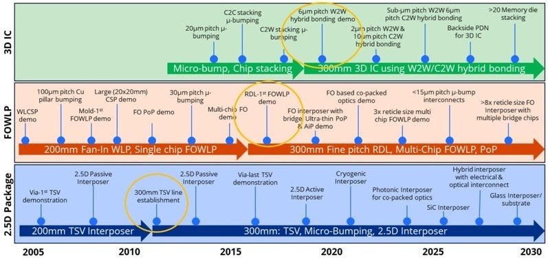
IME has established mature capabilities in Fan-Out Wafer-Level Packaging (FOWLP) and 2.5D/3D IC integration, supporting TSVs, TGVs, chiplet architectures, and thermo-mechanical modeling. These platforms are widely applied in high-speed networking chips, AI accelerators, and Co-Packaged Optics (CPO) modules.
Silicon Photonics & Optoelectronic Integration
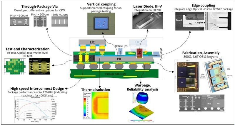
IME is one of the few research institutions in Asia with end-to-end capabilities in silicon photonics process, packaging, and testing. Its Photonic Integrated Circuit (PIC) platform supports components such as Mach-Zehnder Modulators (MZMs), GeSi detectors, and optical couplers. These technologies have already been used to develop 224 Gbps/lane optical engines, positioning IME at the forefront of next-generation data center optical connectivity.
MEMS and Intelligent Sensor Systems
IME has extensive experience in Micro-Electro-Mechanical Systems (MEMS), covering applications from fluid sensing and micro-pressure measurement to biomedical chips. The institute offers an integrated process flow from wafer fabrication to packaging and testing, supporting sensor development across multiple domains.
Compound Semiconductors and Power/RF Devices
IME also develops platforms based on GaN-on-Si, InP, and GaAs for high-power and high-frequency applications. These are critical for emerging 6G communications and power electronics, supporting heterogeneous integration of compound semiconductor components.
End-to-End Integration Capability
IME is among the few institutions in Singapore with both 200mm and 300mm process capabilities. It offers in-house processing from front-end CMOS fabrication to back-end packaging and optical testing. The institute also provides comprehensive support in package reliability simulation (thermal warpage, solder fatigue), signal integrity analysis (S-parameters, eye diagrams), and thermal modeling, meeting the demanding requirements of AI and HPC systems.
Global Collaboration and Technical Influence
IME has longstanding R&D collaborations with leading global companies, including:
Foundries and IC design firms: TSMC, Intel, GLOBALFOUNDRIES, AMD, NVIDIA
Advanced packaging and test houses: ASE, Amkor, JCET
Silicon photonics and optical comms companies: Lightmatter, NTT, Juniper, Rain Tree Photonics
IME regularly presents high-impact research at top international conferences such as IEEE ECTC, OFC, and IEDM, further reinforcing its academic and industrial influence.
Looking Ahead
As AI models scale and computing demands surge, IME’s heterogeneous integration platforms will play a critical role in enabling Co-Packaged Optics, silicon photonic modules, and high-speed memory interfaces (such as HBM + optical engines). With its comprehensive R&D capability “from materials to modules,” IME is positioned to support Singapore’s ambition to become a global hub for advanced packaging and photonic-electronic convergence.

The recent work by A*STAR presents an outstanding advancement by integrating glass interposers into a heterogeneous Co-Packaged Optics (CPO) platform, demonstrating a new level of complexity and performance in optical engine design. In parallel, Broadcom’s Tomahawk 5 (TH5) also leverages Fan-Out Wafer-Level Packaging (FOWLP) to enable high-bandwidth, low-loss integration in commercial switching silicon.
In this article, SemiVision bridges the concepts from both Broadcom and A*STAR, drawing connections between their packaging philosophies and exploring the broader implications of heterogeneous integration in next-generation optical systems. A key focus of this comparative analysis is the impact of different vertical interconnect technologies—TSV (Through-Silicon Via), TGV (Through-Glass Via), and TMV (Through-Mold Via)—on insertion loss performancein high-frequency environments.
By examining how each approach affects signal integrity, especially in the context of AI and HPC workloads, this article offers a comprehensive perspective on the materials, process technologies, and design trade-offs shaping the future of optical engine integration.

For Paid Members,SemiVision will discuss topics on
Design Strategies for Performance and High-Density Integration
Manufacturing and Process Measures for Ensuring Reliability
Broadcom’s Silicon Photonics Packaging Strategy: FOWLP Technology Accelerates Co-Packaged Optics Commercialization
The Role of FOWLP in Silicon Photonics Packaging
Broadcom’s Implementation Case: From Tomahawk 5 Bailly to the Next-Generation Leap with Tomahawk 6
Tomahawk 5: Key Design Highlights and TH5 vs. TH6 Comparison Overview
6.4 Tbps Co-Packaged Optical Engine: A Heterogeneous Integration Platform for AI and Data Center Interconnects
Heterogeneous Integrated Optical Engine: Enabling Co-Packaging from Electronics to Photonics
FOWLP Process and Modular Packaging: Supporting Double-Sided Routing and High-Yield Optical Testing
Through-Glass Via (TGV): A Next-Generation Core Interconnect Technology
Optoelectronic Component Integration: The Core of High-Speed Bidirectional Optical Transmission
Thermal and Reliability Simulation: Enabling Sustained High-Performance Operation

