

UMC’s Strength in the Silicon Photonics Supply Chain
Original Article by SemiVision Research

SemiVision Research previously published a global map of silicon photonics foundries, highlighting key players in the ecosystem. In Taiwan, the primary foundries involved are TSMC and UMC. While we’ve already discussed TSMC’s silicon photonics capabilities extensively, let’s now turn our attention to Taiwan’s second-largest foundry—UMC—and its progress in advanced packaging and silicon photonics.

According to UMC’s special technology roadmap , the company has been deeply involved in the silicon photonics industry for quite some time. Currently, UMC’s silicon photonics production is primarily based on 8-inch wafers, and its major clients are actively pursuing developments in Photonic Integrated Circuits (PIC) and Co-Packaged Optics (CPO).
Taiwanese chipmaker UMC denies merger talks with GlobalFoundries
According to a report by Nikkei Asia, U.S. chipmaker GlobalFoundries and Taiwan’s second-largest chipmaker United Microelectronics Corporation (UMC) are exploring the possibility of a merger. This move is seen as a measure by the United States to mitigate risks associated with the Taiwan Strait while also countering China’s increasing competition in the mature process chip sector.
The evaluation plan indicates that the merged company would become a large enterprise headquartered in the United States, with production facilities spanning Asia, the U.S., and Europe. The purpose of the merger is to establish a company with economies of scale, ensuring a stable supply of mature process chips for the U.S. amid rising tensions between China and Taiwan, as well as China's efforts to strengthen its domestic chip production.

Even After the “GlobalFoundries-UMC Merger,” They Remain the No.2 Foundry
Following the news, UMC’s stock price soared over 14% during Monday's U.S. ADR trading, closing at $7.15 with a gain of 9.16%, marking its highest level since November 8, 2024.
According to data from Companies Market Cap, UMC's current market capitalization has reached $18.42 billion (approximately NT$612.4 billion), ranking 1,029th globally. Meanwhile, GlobalFoundries has a market capitalization of $20.4 billion (approximately NT$677.9 billion), ranking 952nd globally.
According to a SemiVision report, in the global foundry industry, UMC holds a 5.8% market share, ranking third, while GlobalFoundries ranks fifth with a 5.5% market share. Together, the two companies' combined market share is approximately 11.3%.
If the merger succeeds, the newly combined entity is expected to surpass Samsung Electronics’ 11% market share and SMIC’s 5.7% to become the world’s second-largest foundry. However, it would still lag far behind the industry leader TSMC, which commands a dominant 65% market share.
GlobalFoundries Discusses U.S. Manufacturing
GlobalFoundries CEO Thomas Caulfield has emphasized that U.S. tariffs on foreign-made chips could benefit domestic semiconductor manufacturers by increasing demand for locally produced chips. Speaking at a Morgan Stanley investor conference, Caulfield highlighted that while the $52.7 billion CHIPS and Science Act and investment tax credits have enhanced U.S. chip-making capacity, the implementation of tariffs would further encourage companies to source semiconductors domestically.
Caulfield stated, "You need the CHIPS Act and investment tax credits to build capacity, but you need tariffs to create the demand dynamics that bring manufacturing back to the U.S."
These remarks coincide with reports that GlobalFoundries and Taiwan's United Microelectronics Corporation (UMC) are exploring a potential merger. Such a merger would create a larger U.S.-based chipmaker with a global manufacturing footprint across Asia, the U.S., and Europe. This development aligns with U.S. efforts to strengthen its semiconductor supply chain amid geopolitical tensions and increasing competition from China in the mature chip market.
These developments highlight the strategic measures being considered to bolster the U.S. semiconductor industry and reduce reliance on foreign chip production.
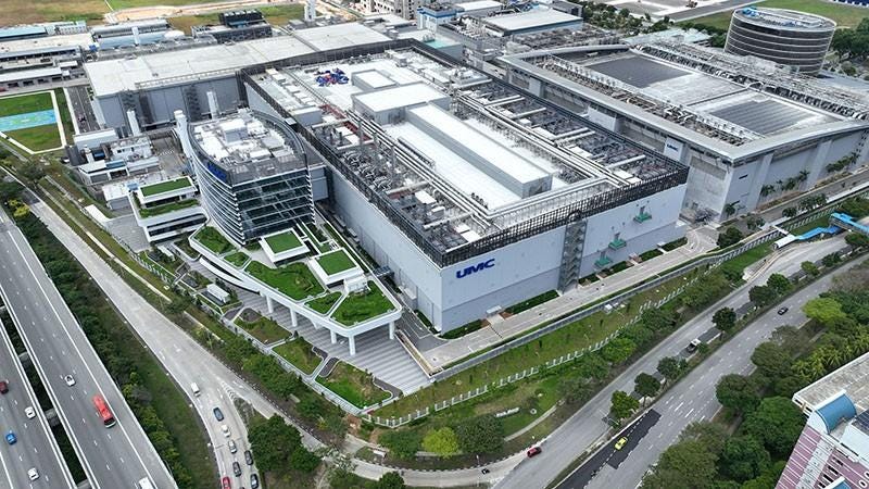
UMC Unveils New Fab Expansion in Singapore in Grand Opening Ceremony
UMC’s New Singapore Fab Offers 22nm and 28nm Process Technologies
UMC stated that its new fab in Singapore will provide industry-leading 22nm and 28nm process technologies, making it the most advanced foundry process in Singapore’s semiconductor industry. It will serve global customers by supplying high-performance chips for advanced smartphone displays, IoT devices, and next-generation communication chips.

Discussing the plans for the new Fab12i facility, UMC emphasized that its design incorporates stringent sustainability standards and has received the GoldPlus certification from the Singapore Building and Construction Authority (BCA) Green Mark. This aligns with UMC’s design standards for all new fabs.
Additionally, 17,949 square meters of solar panels will be installed on the fab’s rooftop, supporting UMC’s goal of achieving 100% renewable energy usage by 2050.
UMC’s Strategic Deployment in Silicon Photonics and Advanced Packaging: Evolving from Mature Nodes to a Pillar of Heterogeneous Integration
As AI, high-performance computing (HPC), and high-speed communication technologies continue to advance rapidly, heterogeneous integration is becoming a key direction in chip design and manufacturing. Traditional foundries are no longer expected to solely provide logic process capabilities—they must now be able to integrate photonic components, memory modules, high-speed I/Os, sensors, and advanced packaging interconnects. UMC is actively responding to this industrial shift through comprehensive deployments across its 8-inch and 12-inch wafer platforms, positioning itself as a crucial enabler for next-generation system architectures.
UMC leverages its strength in mature node manufacturing through its 8-inch fabs, which not only offer cost and process stability but also serve as hubs for specialized process innovation. Notably, UMC has successfully introduced silicon photonics (SiPh) processes on its 8-inch platform, creating a scalable photonic integration foundation for future interconnect technologies such as CPO (Co-Packaged Optics) and OIO (Optical I/O). In parallel, UMC is actively expanding into MEMS (Micro-Electro-Mechanical Systems), supported by a dedicated development team focused on acoustic, pressure, and optical MEMS structures—paving the way for broader applications in sensing and smart edge devices. UMC’s experience in silicon photonics dates back to 2010, indicating deep know-how in the field. Looking ahead, the company plans to leverage its Fab 12i in Singapore as a development hub for 12-inch silicon photonics, addressing the growing demand for larger wafer integration.
In the area of advanced packaging, UMC has made forward-looking investments to meet the long-term needs of heterogeneous integration. Both its 8-inch and 12-inch lines are equipped with essential tools for backend integration, including SPTS’s Deep Reactive Ion Etching (DRIE) systems to enable Through-Silicon Via (TSV) processing. TSV is a fundamental technology for constructing 3D ICs, 2.5D interposers, and high-bandwidth memory (HBM) modules, directly impacting packaging efficiency, thermal management, and signal integrity. Furthermore, UMC has implemented Wafer-on-Wafer (WoW) bonding techniques in its advanced packaging roadmap. One highlighted application is in RF component packaging, where UMC adopts fusion bonding technology, and serves major customers in the RF domain (specific names confidential or pending disclosure).
Particularly notable is UMC’s Fab 12i in Singapore, which is becoming a strategic node in the global advanced packaging supply chain. According to industry sources, NVIDIA is actively collaborating with UMC through co-sign tooling projects, aimed at qualifying manufacturing capability for interposer fabrication in CoWoS (Chip-on-Wafer-on-Substrate) architectures. This collaboration reflects NVIDIA’s strategic interest in expanding its advanced packaging capacity beyond TSMC and into diversified supply chains—while also validating UMC’s growing role in high-bandwidth interconnect ecosystems.
In summary, UMC is evolving from a traditional logic foundry into a vital enabler of heterogeneous integration, through the deepening of its mature-node platform and the reinforcement of its advanced packaging capabilities. As AI and optical interconnect technologies become increasingly prevalent in data centers and edge systems, manufacturing platforms that integrate silicon photonics, MEMS, TSV, and heterogeneous packaging will serve as essential bridges connecting compute, memory, and communication. UMC’s ongoing strategic investments are positioning the company at the forefront of this transformation—staking its claim in the next generation of chip integration paradigms.

For Paid Member, SemiVison Research will discuss following topics:
UMC’s Strength in the Silicon Photonics (SiPh) Supply Chain
Introduction: The Growing Importance of Silicon Photonics
Overview: What is TFLN?
Ecosystem and Foundry Adoption
Electronic Integrated Circuit (EIC)—>Next generation :SiGe BiCMOS
OFC50: Marvell Demo New optical concepts
Leveraging Advanced Packaging for High-Performance SiPh Modules
UMC’s Readiness for Silicon Photonics
UMC’s 12” Advanced Packaging Capabilities
UMC’s Path to Becoming a SiPh Powerhouse
UMC Silicon Photonic Ecosystem

2025 GTC Review: The Silicon Photonics Era Has Arrived – Get Ready!
2025 Nvidia GTC Preview: Insights into Nvidia’s AI Ecosystem
Nvidia GTC AI Conference Preview: GB300, CPO switches, and NVL288
TSMC and NVIDIA Pioneering the Future of AI with Silicon Photonics Technology
CPO Switch Technology Analysis
How to Distinguish Between CPO and OIO? What Is Their Fundamental Difference?
How TSMC’s Silicon Photonics Could Impact NVIDIA’s Future
NVIDIA x TSMC: A Milestone in Silicon Photonics and Optical Integration
TSMC Silicon Photonic Ecosystem
Nvidia Silicon Photonic Ecosystem
Taiwan Silicon Photonic Ecosystem
UMC Silicon Photonic Ecosystem
Global Silicon Photonic Ecosystem
Marvell Silicon Photonic Ecosystem
Broadcom Silicon Photonic Ecosystem