Next-Gen Optics Need Next-Gen Materials: CPO Challenges and the Path Forward
Original Article by SemiVision Research (TSMC , Nvidia , Henkel ,Celestial AI ,NewPhotonics,FiconTEC ,Suruga Seiki,Teradyne,Lightwave Logic,NLM Photonics,Panasonic,Kyocera,Daikin)

Over the past few articles, SemiVision has extensively explored the evolving landscape of silicon photonics, with particular emphasis on the technological roadmaps of TSMC and NVIDIA. Our analysis has underscored the foundational role of silicon photonics in enabling both scale-up and scale-out across next-generation AI and data center architectures.
For example, Celestial AI’s Photonic Fabric represents a groundbreaking architectural innovation, leveraging photonic interconnects as a system-level fabric for memory and compute. SemiVision is currently preparing a dedicated feature report on Celestial AI, exploring its design principles and ecosystem implications.

Looking ahead, we see a clear trend toward heterogeneous integration of light sources directly within photonic systems—sometimes referred to as the Optical Signal Processor (OSP) model. This reflects the direction of companies like NewPhotonics, which are building next-generation platforms where optical compute and signal processing are tightly co-optimized.
In the critical domain of optical coupling and alignment, Suruga Seiki of Japan has proposed a highly refined and complete solution stack. Their systems support sub-micron active alignment precision, essential for reliable coupling between fiber arrays and photonic integrated circuits (PICs), especially under thermal and mechanical constraints in CPO environments.

On the manufacturing and testing front, FiconTEC of Germany stands out with a vertically integrated supply chain for photonic and electronic IC (EIC + PIC) test and assembly. Their ecosystem spans from high-precision die bonding to automated optical alignment, active testing, and backend packaging. Notably, at the upcoming Laser World of Photonics trade fair in Munich (June), FiconTEC is set to unveil its latest advancements, including double-sided photonic device testing systems.


Moreover, FiconTEC has entered into a strategic collaboration with Teradyne, combining their optical alignment and packaging expertise with Teradyne’s strength in high-throughput, wafer-level test automation. This partnership aims to address the scalability, reliability, and cost-efficiency challenges of mass-producing photonic-enabled AI hardware.

Beyond integration architectures, we’ve also addressed material innovation in photonic devices—highlighting, for instance, Lightwave Logic’s polymer-based electro-optic modulators as a disruptive alternative to conventional silicon-based designs. In parallel, NLM Photonics has been actively developing cutting-edge solutions, collaborating closely with partners in Taiwan to co-develop the next generation of silicon photonics technologies.


Furthermore, there has been growing interest in TFLN (thin-film lithium niobate) platforms within industry forums, with discussions centered on how to align such high-performance photonic materials with standard CMOS process flows. However, one critical element often overlooked is the importance of packaging and interfacial materials—particularly adhesives and encapsulants used in silicon photonics modules.
These materials are not simply passive fillers—they play a pivotal role in:
Maintaining optical alignment and mechanical stability
Managing thermal dissipation
Ensuring long-term environmental reliability
Among the key players in this space, Henkel stands out with a broad portfolio of optical-grade adhesives, die attach films, capillary underfills, and thermal interface materials tailored for CPO (Co-Packaged Optics) and silicon photonics applications.

This article will take a deeper look at:
The material-level challenges faced by CPO packaging, especially under tight thermal, optical, and mechanical constraints
Material-based solutions engineered for these environments, including high-thermal adhesives, low-CTE underfills, and phase-change TIMs
A landscape of leading suppliers—from Henkel to specialized material innovators—who are enabling the future of silicon photonics through advanced packaging chemistry
By shedding light on this often-underappreciated layer of the CPO ecosystem, we aim to bridge the gap between photonic design and material science—an essential step in realizing scalable, reliable, and thermally efficient optical-electrical convergence.
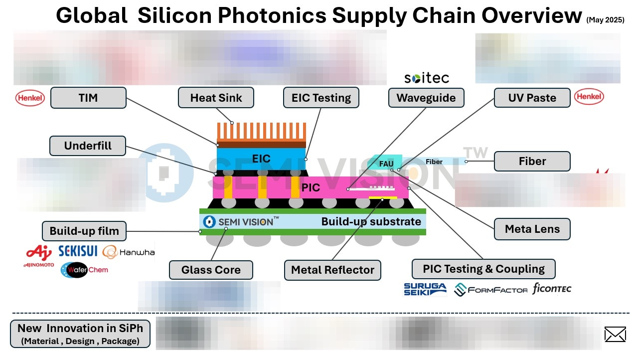
As data centers continue to evolve, Co-Packaged Optics (CPO) technology is gradually replacing traditional pluggable optical modules, emerging as a cornerstone of next-generation high-performance computing and AI infrastructure. By directly integrating optical components—such as lasers and photodetectors—into the same package as switch ASICs or XPUs, CPO significantly shortens the distance between electrical and optical signal domains. This enables higher bandwidth density, reduced latency, and improved energy efficiency.
However, the adoption of CPO also introduces unprecedented challenges in materials engineering and thermal management. The integration of high-power lasers, the thermal sensitivity of optoelectronic components, and the increased thermal crosstalk inherent in high-density packaging all impose stringent requirements on materials in terms of thermal conductivity, mechanical stability, and photonic alignment precision. As a result, selecting the right packaging materials has become a critical enabler for the commercialization and scalability of CPO technology.
The following introduces three essential materials for CPO (Co-Packaged Optics) packaging and explains how each plays a vital role in overcoming the aforementioned challenges—enabling data centers to move toward higher performance and greater energy efficiency in the optical-electrical integration era.
UV Optical Adhesive & Supply chain
What is UV-curing resin?
This is a material that "polymerizes and cures in a short time by the energy of ultraviolet rays (UV) emitted from an ultraviolet irradiation device".

UV-curing resins are roughly classified into two major types: acrylic resins and epoxy resins. While both types are cured through exposure to ultraviolet (UV) light, they differ significantly in their curing mechanisms, performance characteristics, and end-use applications.

Acrylic resins undergo radical polymerization, a chain reaction initiated by UV light that activates photoinitiators. This reaction proceeds rapidly, making acrylic-based UV resins suitable for high-speed production lines. They typically offer excellent flexibility, good adhesion to a variety of substrates, and low shrinkage, but may be sensitive to oxygen inhibition at the surface, which can affect surface cure.

In contrast, epoxy resins cure via a cationic polymerization mechanism when exposed to UV light. This method is less affected by oxygen inhibition, resulting in better surface hardness and chemical resistance. Epoxy UV resins also have superior thermal stability and moisture barrier properties, making them ideal for electronics, optical components, and structural bonding applications. However, their curing speed is generally slower than acrylics, and they often require post-curing via heat to achieve full cross-linking and performance.

Choosing between these two resin types depends on the specific requirements of the application — such as cure speed, mechanical strength, environmental resistance, and substrate compatibility. Understanding these differences is essential when designing processes for advanced packaging, coatings, adhesives, or encapsulation in microelectronics and photonics.
Application Characteristics:
Designed for precise photonic alignment, ensuring high-accuracy coupling between optical fibers and photonic chips.
Exhibits high transmittance at 1310nm and 1550nm, with low shrinkage and anti-fog properties, making it ideal for long-term, stable optical connections in CPO modules.
In photonic modules, the Fiber Array Unit (FAU) is typically connected to the Photonic Integrated Circuit (PIC) through a passive-active alignment process. After precise alignment is achieved, UV-curable resin is applied to secure the FAU to the PIC, ensuring long-term optical alignment stability.
However, several key issues must be considered:
Coefficient of Thermal Expansion (CTE) Mismatch: The difference in CTE between the UV resin and the glass or silicon substrates can introduce mechanical stress during thermal cycling, potentially causing interface delamination or optical misalignment.
Non-uniform Curing: In V-groove structures, UV light may not evenly penetrate the adhesive layer, leading to under-cured areas that increase the risk of interface separation.
Moisture Absorption and Aging: Some UV resins are hygroscopic and may absorb moisture over time, which can degrade optical performance or lead to material deterioration.。
Key Suppliers and Products:
Dymax: The OP series (e.g., OP-29, OP-29-GEL) offers fast UV curing, low shrinkage, and excellent optical clarity, making it well-suited for fiber array assembly and securing optical components in high-precision applications.

Norland Products: The NOA series (e.g., NOA 138) consists of single-component UV-curable adhesives with outstanding optical properties and strong adhesion, widely adopted for photonic element bonding and lens attachment in optoelectronic packaging.

Daikin: Its OPTODYNE series is based on fluorinated epoxy resins and is specifically designed for high transparency and refractive index matching in optical component applications.

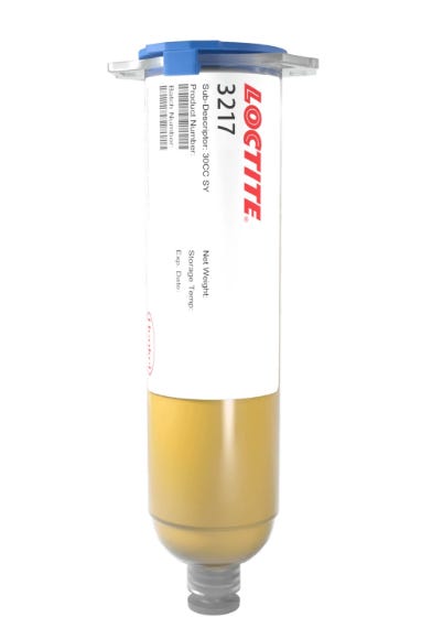
Henkel LOCTITE® AA 349 / Henkel LOCTITE® 3217

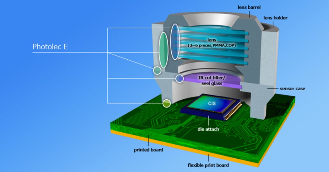
Sekisui: UV Delayed-Cure Low-Permeability Adhesive – Photolec E Series
This UV-curable adhesive is designed for rapid bonding of optical components to substrates under low-temperature conditions. Product Features as below:
Delayed UV curing: Begins to cure a few minutes after UV exposure, allowing for post-alignment. Final curing is achieved through brief low-temperature heating, enabling rapid internal curing.
Low outgassing: Exhibits high moisture vapor barrier performance and minimal emissions.


These UV optical adhesives form the backbone of robust photonic integration, enabling the alignment stability and optical clarity required in high-density CPO environments.
Supply Chain Challenges and Market Trends
In recent years, the supply chain for UV optical adhesives has faced multiple challenges:
Raw Material Price Volatility: The prices of key raw materials such as photoinitiators, oligomers, and monomers are affected by geopolitical tensions, environmental regulations, and supply chain disruptions, leading to rising production costs.
Supply Chain Disruptions: Events such as natural disasters, trade disputes, and global health crises have impacted the availability of raw materials and components.
High Entry Barriers: The production of UV-curable optical adhesives requires specialized equipment and technical expertise, posing a significant challenge for new market entrants.
Henkel Semiconductor Materials Portfolio Overview


For Paid Members, SemiVision will discuss topics on
Liquid Molded Underfill (MUF) & Supply Chain
High-Thermal Capillary Underfill (CUF) & Supply Chain
Modulus at Elevated Temperature — A Core Indicator of Thermo-Mechanical Stability
Global Supply Chain Overview of Critical Semiconductor Packaging Materials
Current Status and Outlook of the Global Silicon Photonics Industry (2025,05)