

Semiconductor IC Testing: A Comprehensive Analysis from Core Processes to Advanced Packaging Challenges
Original Article by SemiVision Research (TSMC , Nvidia , Advantest , Teredyne , KLA, Onto , Camtek, Nova , FiconTEC ,Chroma, Cohu)

Semiconductor IC Testing: From Fundamental Processes to New Challenges in Advanced Packaging and the Silicon Photonics Era
In the past, IC testing in semiconductor development was largely regarded as a standard procedure following fabrication. For traditional logic chips, the testing flow typically involved wafer sort, post-package ATE (Automatic Test Equipment) testing, burn-in, and final product verification. While these steps were complex and time-consuming, they were still considered relatively fundamental tasks aimed at filtering defects and ensuring yield.
However, with the rise of AI chips, 3D ICs, and heterogeneous integration, testing has evolved into a critical pillar that directly impacts cost, reliability, and co-optimization with design rules. It is increasingly recognized as the next frontier of industry competition.
From Conventional to Advanced Nodes: Coupling Tooling Rule and Packaging Design Rules
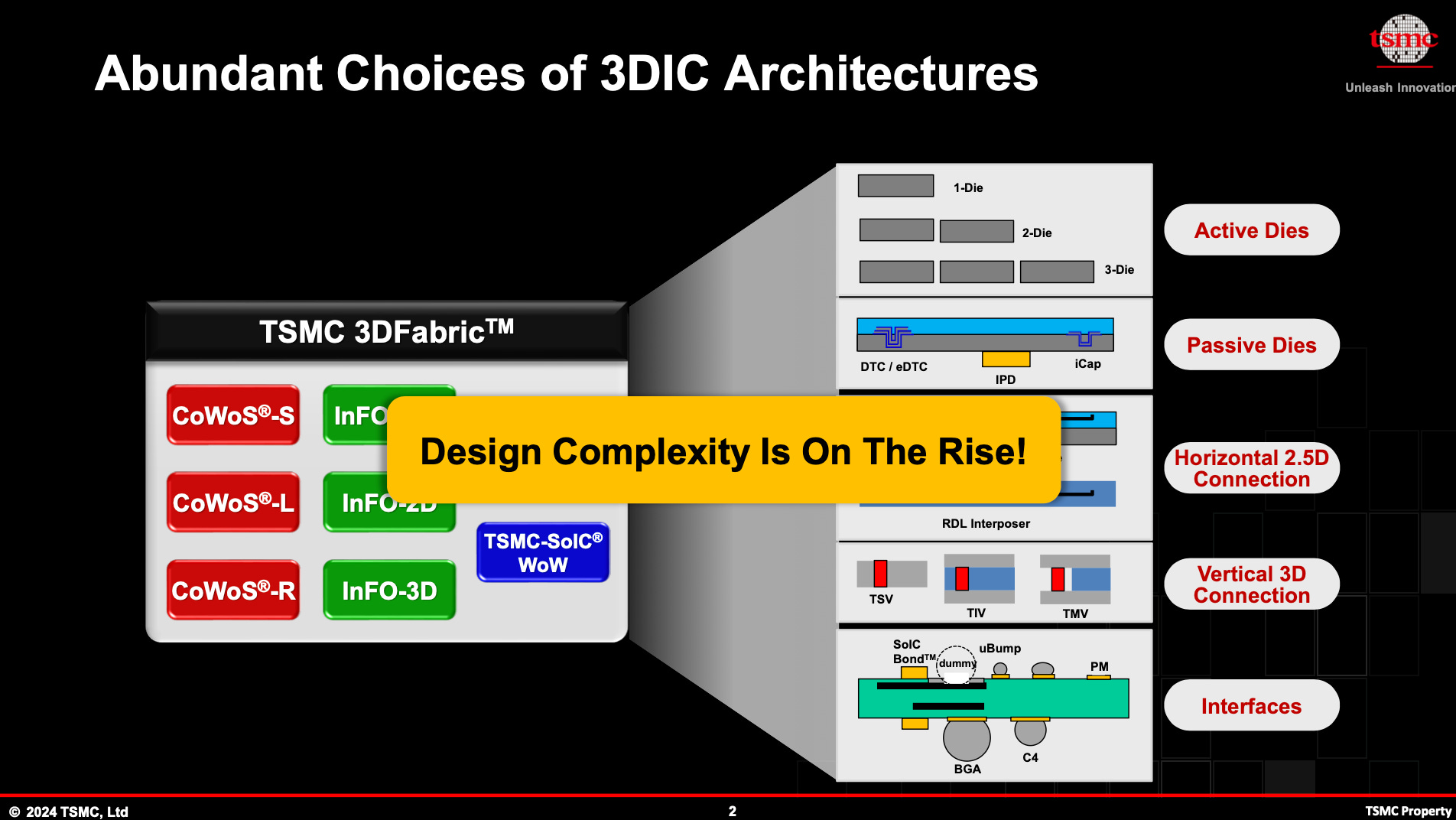
Today, advanced process nodes and advanced packaging are no longer viewed in isolation. When customers evaluate Tooling Rule , they must also consider compatibility with advanced packaging approaches such as 2.5D/3D IC, chiplet, and SoIC architectures. In such system designs, it is not only circuit routing that must comply with design specifications—power distribution networks (PDN), signal integrity (SI), and power integrity (PI) must also be co-optimized. Otherwise, unpredictable failures may arise under high-speed, high-frequency operation.
To address this, foundries such as TSMC have introduced dedicated 3D IC design rules, requiring customers’ designs to operate within a defined process window in order to clarify accountability. However, many system companies often prefer to “stretch the rules” in pursuit of maximum performance. This not only tests the flexibility of foundry processes but also elevates the role of testing, making it critical for both early-stage validation and high-volume manufacturing.
Expanding Test Coverage and Reliability Requirements
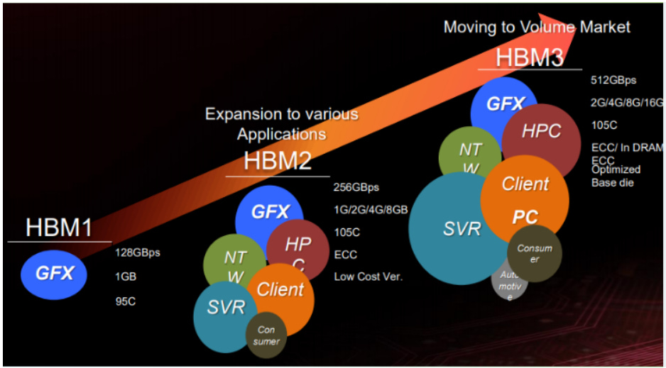
With rising frequencies and data rates, test coverage has gone far beyond conventional DC tests and functional verification. Greater emphasis is now placed on high-speed interfaces, high-frequency signal integrity, and long-term reliability. For AI chips, which incorporate massive SerDes links, HBM stacked memory, and complex chiplet interconnects, testing methodologies must validate high-speed links, power transients, and cross-die signal transmission.
At the same time, reliability testing requirements have grown significantly, encompassing high-temperature operating life (HTOL), high-voltage stress, thermal cycling, and mechanical stress tests. These measures ensure that products can operate stably over extended lifespans in demanding environments such as data centers and automotive electronics.
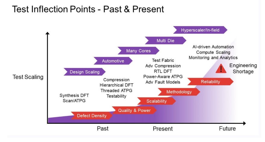
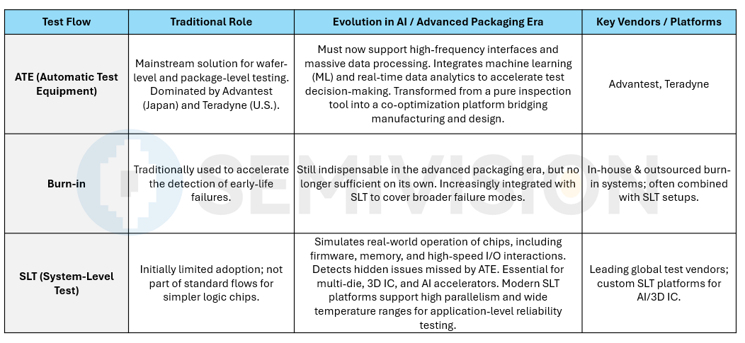
The Evolving Roles of ATE, Burn-in, and SLT
ATE (Automatic Test Equipment): Traditionally the primary solution for wafer-level and package-level testing, dominated by Japan’s Advantest and the U.S.’s Teradyne. With the acceleration of AI chips, ATE must now support high-frequency interfaces and massive data processing, while integrating machine learning (ML) and real-time data analytics to enhance test decision speed. As a result, ATE has transformed from a pure inspection tool into a critical platform for co-optimization between manufacturing and design.
Burn-in: Historically used to accelerate the screening of early-life failures. While still indispensable in the advanced packaging era, Burn-in alone can no longer capture all failure modes and is therefore increasingly integrated with system-level test (SLT).
SLT (System-Level Test): Simulates real-world chip operation, covering interactions among firmware, memory, and high-speed I/O. SLT is capable of identifying latent issues that ATE cannot capture. For multi-die, 3D IC, and AI accelerators, SLT has become an essential stage. Leading global test vendors have introduced SLT platforms that support high parallelism and wide temperature control, bringing reliability testing closer to actual application conditions.
In modern test strategies, a common approach is “Shift Right + Shift Left”: first capture system-level failures through SLT, then feed the failure modes back into ATE and design rules, creating a closed-loop optimization cycle.
Testing supply chain and major suppliers
The semiconductor test supply chain remains dominated by a handful of giants. Japan’s Advantest virtually monopolizes ATE supply for AI and advanced-node chips, while Teradyne is rapidly expanding in SLT and parallel testing. Supporting equipment such as handlers and probers is largely dominated by Japanese firms such as TEL and Tokyo Seimitsu. This high concentration of the supply chain makes advanced chip testing resources increasingly strategic. Together, Advantest and Teradyne account for more than 70% of the global ATE market.
Chroma has achieved strong penetration and rapid growth in Asian markets, particularly in Taiwan and China.
Cohu (including Xcerra and LTX-Credence) holds a position in the market by offering a comprehensive “ATE + Handler” solution.
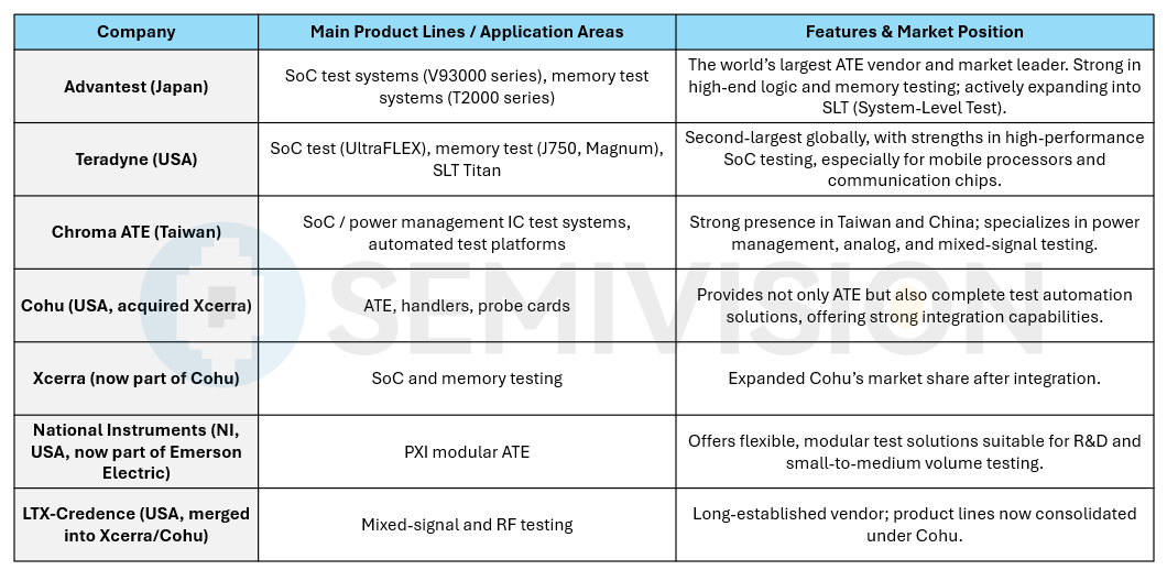
Meanwhile, regional players in China and Southeast Asia are emerging in niche markets such as automotive and consumer IC testing, presenting new competition to the international leaders.
In this article, our focus will be on key challenges in semiconductor testing and an analysis of testing methodologies. We will also provide a basic overview of the upstream, midstream, and downstream segments of the supply chain.
In semiconductor manufacturing, Wafer Acceptance Test (WAT) and Process Control Monitor (PCM) are critical quality checkpoints conducted after wafer fabrication. By measuring multiple monitoring structures, they evaluate both across-wafer and intra-wafer electrical distributions, providing customers with essential data to assess process uniformity and yield. At the same time, fabs also perform QA defect density inspections to ensure products meet specifications before proceeding to subsequent processes or shipment. Traditionally, this stage marked the “end point” of a foundry’s responsibility. However, with the rise of advanced packaging, it has increasingly evolved into the “starting point” of the packaging process.
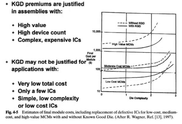
Before entering advanced packaging technologies such as CoWoS, SoIC, or InFO, Known-Good-Die (KGD) screening is mandatory to prevent defective dies from being stacked, which would otherwise result in costly rework. At the same time, the industry has placed greater emphasis on testing interposers and substrates, including RDL formation quality, micro-bump coplanarity, and defect detection. These checks must be implemented at mid-process stages through AOI and electrical testing to avoid defects propagating into final assemblies. Therefore, the true “starting point” of advanced packaging is not only KGD but also yield assurance for interposers and substrates, ensuring stability in subsequent integration.
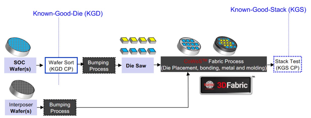
At the CoWoS/SoIC packaging stage, testing focuses on the electrical and reliability characteristics of RDL traces, TSVs, and micro-bumps. Test structures such as daisy-chain, Kelvin, via-chain, and meander patterns are used to validate continuity and RC characteristics, while reliability is assessed under accelerated stress conditions like thermal cycling and baking. Micro-bumps, in particular, require close attention to Joule heating under high current density and coplanarity issues, which are common failure sources. With increasing packaging density and a surge in interconnect counts, both test complexity and cost are escalating significantly.
With the introduction of silicon photonics and co-packaged optics (OIO/CPO), testing challenges rise further. Optoelectronic integrated components must undergo not only electrical testing but also optical characterization, including insertion loss, extinction ratio, coupling efficiency, and electrical parameters such as BER, eye diagrams, and aging performance. This demands test platforms capable of supporting optical fixtures, precision alignment processes, and system-level correlation testing for thermal drift and long-term aging. Measurement uncertainty must also be incorporated into guardbands to avoid misjudgments. These requirements highlight why traditional logic testing methodologies are no longer sufficient to meet future demands.
In GPU and HBM high-bandwidth integration, signal integrity (SI) and power integrity (PI) have become critical factors for system-level optimization. By strengthening the power delivery network (PDN), increasing metal thickness, and adopting advanced RDL designs (such as eDTC technology), jitter and power consumption in high-speed data transmission can be effectively reduced. The linewidth, spacing, and layout of RDL have significant impact on SI/PI, requiring close coordination across design, packaging, and testing stages.
Meanwhile, the acceleration of SerDes and PCIe introduces new challenges. For example, in PCIe 7.0, operating at 32 GHz, channel loss, jitter, and BER specifications are far more stringent. To meet these requirements for high-speed serial links, server motherboards must employ ultra-low Dk/Df materials such as Megtron 7 or Tachyon. This means that testing must extend beyond IC-level validation and be closely integrated with PCB material choices and system design, forming an end-to-end testing methodology.
In summary, the role of testing has evolved from being the “end point of wafer-level inspection” to the “starting point of advanced packaging,” and is now progressing toward the “core of system design and packaging integration.” This progression spans wafer-level WAT/PCM and QA, KGD and interposer screening, CoWoS/SoIC packaging tests, silicon photonics and optoelectronic integration, as well as system-level validation of GPU × HBM and SerDes/PCIe. By strengthening interposer screening and optical-electrical measurement planning, this holistic testing framework can serve as an internal standard, enabling designers, foundries, OSATs, and testing teams to collaborate effectively and ensure quality and reliability from process to system.
SemiVision has conducted an in-depth analysis of the current inspection and testing supply chain, covering key suppliers in Inline Inspection. Leading players include KLA (optical and e-beam inspection and metrology platforms), Onto Innovation (optical defect inspection, overlay, and metrology solutions), Camtek (wafer AOI and automated packaging inspection), Nova (optical metrology and material characterization), and Hitachi High-Tech (SEM and metrology equipment). Together, these companies form a comprehensive ecosystem for inspection and metrology across different stages of wafer process control and defect detection.


In the areas of Failure Analysis (FA), Material Analysis (MA), and Reliability Analysis (RA), the article also introduces widely used techniques. For example, TEM (Transmission Electron Microscopy) is used for nanoscale lattice and defect observation; SEM (Scanning Electron Microscopy) is applied for surface morphology and cross-sectional structure analysis; FIB (Focused Ion Beam) enables precision cross-section preparation and circuit modification; and SIMS (Secondary Ion Mass Spectrometry) allows depth profiling and dopant concentration analysis. For advanced packaging, Acoustic Microscopy is used to detect voids and delamination inside packages, while TSV and 3D IC structures often require X-ray and CT (Computed Tomography) for observing buried structures and interconnect integrity.
The article further extends to new challenges in silicon photonics and optoelectronic testing, including the measurement of optical parameters such as insertion loss, extinction ratio, and coupling efficiency, as well as high-speed driver and TIA eye diagram and BER testing. It emphasizes that traditional logic testing methodologies are insufficient for the demands of photonic-electronic integration. Finally, SemiVision also reviews foundational testing concepts—from CP (chip probe/wafer test), FT (final test), to SLT (system-level test)—along with the introduction of modern testing strategies such as Part Average Testing (PAT) and Adaptive Test (AT), providing readers with a complete view of the semiconductor testing and inspection ecosystem.
This article will serve as a must-read reference for anyone seeking to understand the full chain from wafer processing and packaging to system-level testing. Whether the focus is on the equipment supply chain for industry analysis or the technical depth needed by engineers, readers will find substantial value.
SemiVision has pointed out that future design will move toward chiplet architectures, which means the complexity in testing will only continue to increase. SemiVision recommends that readers who are interested in chiplets consider attending this seminar.
NHanced Semiconductors & University of Florida to Present Chiplet Paper at 36th Electronics Packaging Symposium Held at GE’s Aerospace Research Campus
NISKAYUNA, NY (August 19, 2025) – At the upcoming 36thElectronics Packaging Symposium, held September 3 – 4, 2025, NHanced Semiconductors and a team from the University of Florida will present a technical paper – “The Future of Electronics Packaging: Chiplet Architecture and AI Defect Inspection” – describing how copper-to-copper hybrid bonding enables chiplet interfaces at sub-10µm pitches to increase interconnect densities in advanced packaging assemblies.
NHanced vice-president Dr. Charles Woychik will present the paper, co-authored with U F’s Pavanbabu Arjunamahanthi, et al. from the Department of Electrical & Computer Engineering, during the Symposium’s session on Heterogeneous Integration.
The paper examines the emerging chiplet ecosystem including process architectures, integration flow, and fabrication challenges associated with hybrid bonding for chiplet-to-wafer packaging. Also included are standardization trends, such as Universal Chiplet Interconnect Express (UCIe), that guide the development of scalable, high-yield chiplet integration platforms.
According to Woychik, “Hybrid bonding has emerged as a leading solution for fine-pitch die-to-die chiplet integration with robust electrical, mechanical, and thermal continuity. These characteristics are particularly beneficial in chiplet architectures for high performance computing.”
The 36th Annual Electronics Packaging Symposium will be held at the GE Aerospace Research Center in Niskayuna, NY from September 3 - 4, 2025. The conference is organized by the University of Binghamton’s Integrated Electronics Engineering Center and The Center for Advanced Microelectronics Manufacturing, in conjunction with GE Aerospace and IBM Research. The Symposium is focused on electronic packaging and the evolution of advanced packaging toward a chiplet future. Registration for the event is available here.
About NHanced Semiconductors, Inc.
Based in the US, NHanced Semiconductors is the world’s first pure-play advanced packaging foundry, specializing in leading-edge BEoL semiconductor technologies. Its capabilities include chiplets, 3D-ICs, silicon interposers, 2.5D, additive silicon manufacturing, photonics, microfluidics, and other innovative technologies. The foundry works with both standard and non-standard substrates, III‑V compound semiconductors, and many specialized materials.
Headquartered in Illinois, NHanced has a development and manufacturing facility near Research Triangle Park, NC, performing small volume manufacturing, in-house process development, and customer prototyping, and an advanced packaging and assembly facility in Odon, IN. For more information, please visit:
Media contact:
Chris Burke, BtB Marketing Communications
(919) 637-3510
For Paid Members, SemiVision will discuss topics on
Integration Challenges in Future Silicon Photonics Testing
Exploring in Supply Chain (KLA ,Onto ,Camtek ,Nova….)
Supply Chain Dimensions and Collaboration Workflow
Industry Value Chain and Company Types
Key Stages and Objectives of IC Testing: Step-by-Step Screening from Wafer to System
Wafer Acceptance Test (WAT)
Wafer Probe (CP)
Final Test (FT)
Reliability Testing (R-Test)
Electrical Quality Check (EQC)
System-Level Test (SLT)
Core Test Technologies and Equipment: Bringing ATE Capabilities “Onto” the DUT
Test Specifications and Datasheet Alignment: One Unified Ruler from Design to Production
Common Test Items: Practical Highlights in DC / Functional / AC
DFT and Memory Testing: Designing Testability In
Boundary Scan and High-Speed Interface Testing
Advanced Packaging (CoWoS / SoIC): Dedicated Test Challenges and Countermeasures
Power Semiconductor Testing: High-Voltage/High-Current Measurements and Reliability
Yield Analysis and Data Science: From Patterns to Root Cause
Test Economics and Capacity Operations: Making Every Second Count
ESD/EOS, Power Sequencing, and Failure Prevention: Testing Is Not a Destructive Experiment
Practical Integration of Advanced Packaging: Design—DFT—Packaging—Testing as One
