NVIDIA x TSMC: A Milestone in Silicon Photonics and Optical Integration
Original Articles by SemiVision Research

Before reading this article, we recommend referring to SemiVision Research’s previous coverage on NVIDIA’s silicon photonics and Co-Packaged Optics (CPO) for additional context.
Drive Into Nvidia CPO Based Switch
2025 GTC Review: The Silicon Photonics Era Has Arrived – Get Ready!
2025 Nvidia GTC Preview: Insights into Nvidia’s AI Ecosystem
Nvidia GTC AI Conference Preview: GB300, CPO switches, and NVL288
TSMC and NVIDIA Pioneering the Future of AI with Silicon Photonics Technology
CPO Switch Technology Analysis
How to Distinguish Between CPO and OIO? What Is Their Fundamental Difference?
IEDM 2024: TSMC Silicon Photonics Advancements
TSMC Optical Chiplet Integration and CPO Platform: EPIC-BOE

EPIC=Eletrobic-Photonic chiplet Integration Technology with IC Process
BOE=BroadBand Optical Engine
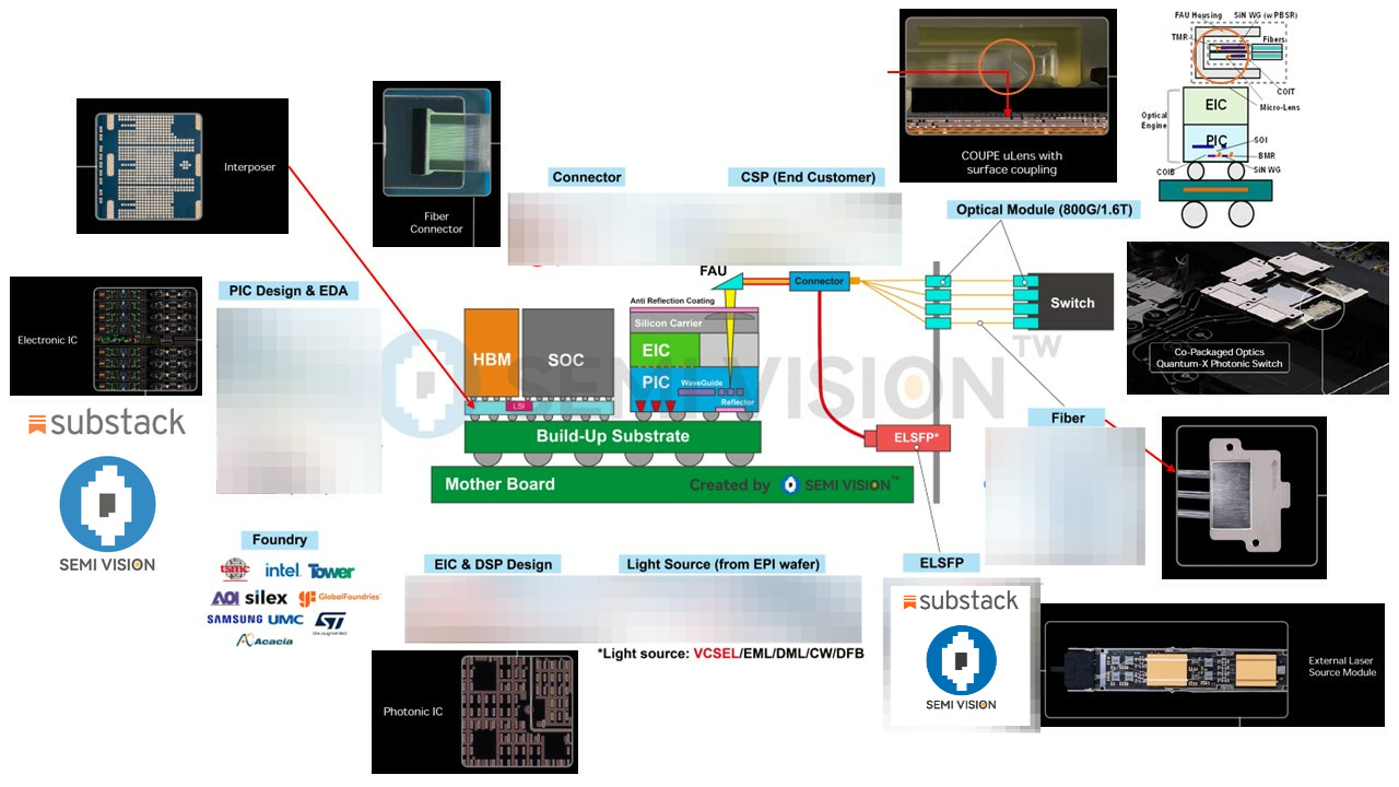
Future GAI systems require much higher parallelism than current architectures, alongside greater energy efficiency, bandwidth density, and lower latency. TSMC proposes EPIC-BOE, a fully integrated technology platform designed for broadband optical engine (BOE) applications. This system enables chip-to-fiber-to-CoWoS level integration and uses TSMC’s 3DFabric and IC process technologies to achieve compact co-packaged optics (CPO), optimizing the PPA (power, performance, area) metrics for GAI systems.
The composition of an Optical Engine (OE) requires two types of dies: the Photonic Integrated Circuit (PIC) and the Electronic Integrated Circuit (EIC), which are fundamentally related to electro-optical conversion.
TSMC, traditionally focused on logic chips — essentially the EIC part — is now actively expanding into the photonics domain, where the PIC component dominates. Recognizing the importance of integrating both photonic and electronic subsystems, TSMC has introduced the COUPE platform and the iOIS (Integrated Optical Interconnection System) platform to bridge these two worlds.
Ultimately, by integrating the entire system from chip to fiber to CoWoS level, TSMC has redefined its silicon photonics strategy with the EPIC-BOE platform — a new benchmark for scalable, high-performance optoelectronic integration.
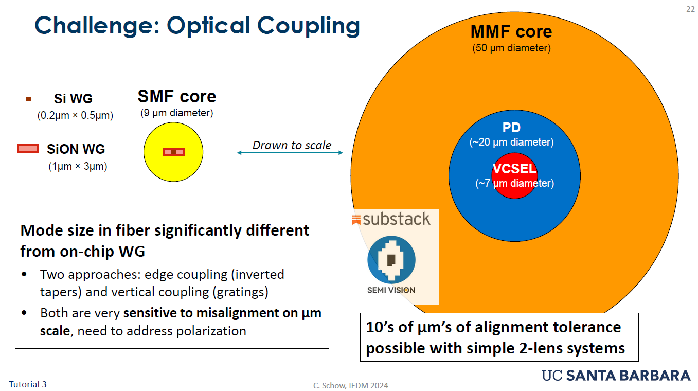
EPIC-BOE supports a wide bandwidth range from 1260 to 1360 nm and integrates vertical couplers capable of supporting high fiber counts. Unlike traditional edge couplers (EC), which are limited by edge warping when integrating 40–80 fibers per row, EPIC-BOE's vertical coupling design eliminates such limitations and allows for multi-row integration.
The process uses IC-based techniques to implement SiN waveguides, optical couplers, interlayer transitions, and polarization control devices. The waveguide propagation loss is 0.01 dB/cm, with a 90-degree bend loss of just 0.001 dB per turn. The vertical coupler achieves ultra-low coupling loss (0.08 dB) and can sustain high-power laser input (300 mW for 3 hours) without degradation. Interlayer transition loss is 0.015 dB. The polarization diversity PBSR achieves an extinction ratio of 23 dB and 0.3 dB loss across TE/TM modes, enabling compact integration in FAUs.
TSMC is about to publish a new paper highlighting the advantages of SiN waveguides (SiN WG) and their integration into TSMC’s silicon photonics platform.
Photonics Platform Integration
Silicon photonics is transforming integrated optics by enabling scalable, manufacturable optical circuits. Optical coupling—especially from fiber to chip—is a key challenge. Common coupling types are grating couplers (GCs) and edge couplers (ECs). While GCs offer easy alignment for fiber arrays, they suffer from limitations in angle sensitivity, polarization dependence, and bandwidth. ECs, on the other hand, offer better broadband performance but struggle with scaling to multiple fiber rows due to chip edge limitations.
Vertical couplers, as adopted by EPIC-BOE, provide a breakthrough in achieving scalability across fiber count per row, number of rows, and individual fiber bandwidth. The system combines COUPE (platform for photonic engines), COIT (complementary optical interconnect top layer), and iFAU (integrated fiber array unit) to provide broadband, vertically-coupled, multi-row optical I/O.


COUPE (platform for photonic engines)
COIT (complementary optical interconnect top layer)
iFAU (integrated fiber array unit)
iOIS (Intergrated to Advanced Package)
Silicon Photonic Supply chain by SemiVision Research
Keep updated latest information to our Paid Members
TSMC Silicon Photonic Ecosystem
Nvidia Silicon Photonic Ecosystem
Taiwan Silicon Photonic Ecosystem
UMC Silicon Photonic Ecosystem
Global Silicon Photonic Ecosystem
Marvell Silicon Photonic Ecosystem
Broadcom Silicon Photonic Ecosystem
For Paid Members , SemiVision Research will discuss following topics:
Why Is NVIDIA Pushing for CPO Switches? Start with Why
Why Choose CPO Technology?
Technical Architecture of the CPO Switch
An in-depth study of the optical engine design approaches by TSMC and NVIDIA
Introduction to the Key Features of TSMC’s EPIC-BOE Platform
Broadcom vs. NVIDIA: A Comparison of CPO Switch Strategies
Why Is NVIDIA Advancing Micro-Ring Modulators and CPO Technology?

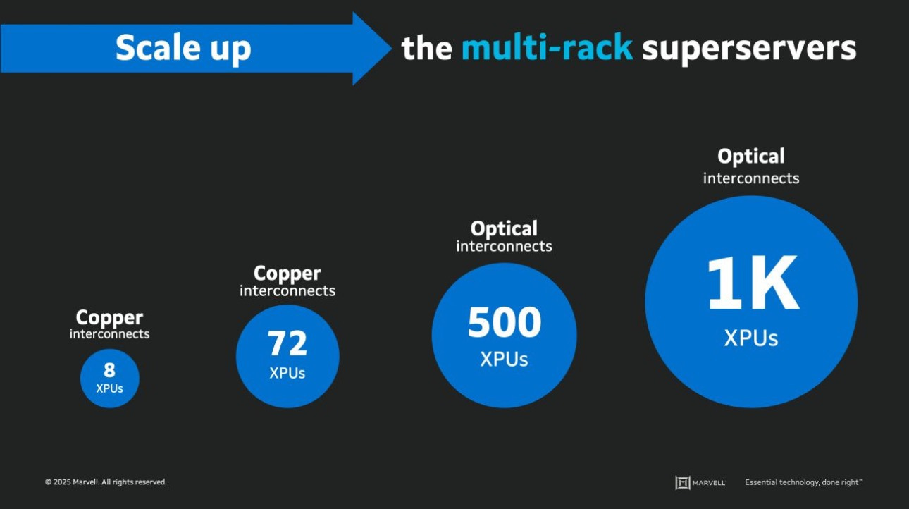
In the architecture of AI Clusters, Scale Out plays a critical role. As a result, Co-Packaged Optics (CPO) technology is destined to become a key development focus. At the same time, with the growing demand for higher-performance GPUs and XPUs, lower latency, and faster data movement, the evolution of AI interconnects is becoming mission-critical.
Scale-up networks are moving beyond traditional copper, transitioning to integrated optics to improve efficiency and speed.
Scale-out networks require resilient, high-bandwidth connectivity to support massive AI clusters.
Silicon photonics innovations are paving the way for CPO technology and next-generation DSPs (Digital Signal Processors), enabling AI infrastructure to scale smarter and faster.