


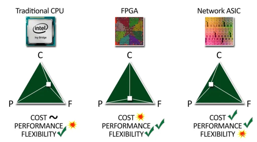
The Rise of ASIC: Custom Chips Becoming a Key Trend!
Comprehensive Analysis of ASIC Players: Broadcom, Marvell, AIchip...

Nvidia's Role in the AI Chip Revolution and the next generation logic device will Shift from 3nm to 2nm
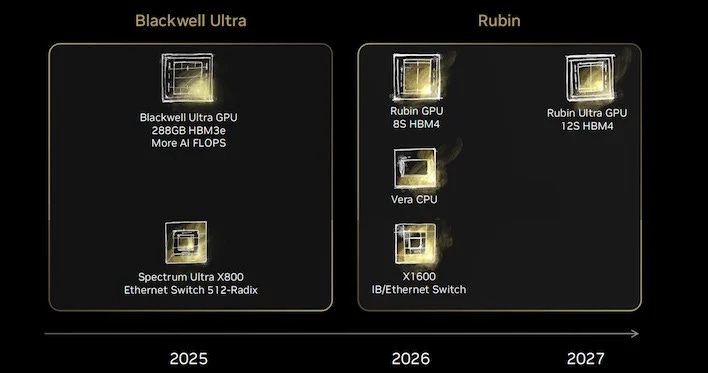
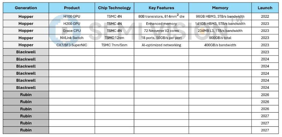
In 2022, Nvidia opened the door to AI chips, positioning itself as the biggest winner in the AI boom. Riding this wave, Nvidia introduced a "one product per year" strategy, launching:
2022: Hopper Platform
2024: Blackwell Platform
2026: Rubin Platform
2027: Rubin Ultra Platform
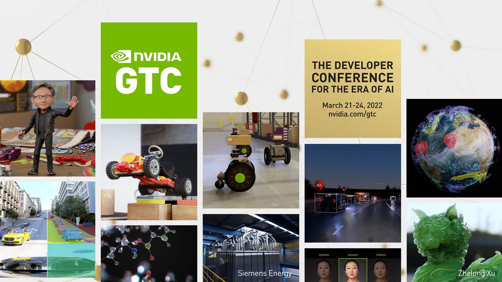
Nvidia GTC AI Conference Preview: GB300, CPO switches, and NVL288

As Nvidia pushes the boundaries of AI chip complexity, it also drives up chip prices, fueling the trend of custom AI chip development. The major ASIC players in this market include Broadcom, Marvell, and others, all of whom share one common factor—their reliance on TSMC’s advanced process nodes.
Currently, TSMC's most advanced node is 3nm, with the next-generation 2nm process on the horizon. The transition from 3nm to 2nm marks a critical inflection point due to structural differences, making the manufacturing process more complex and expensive.
According to SemiVision’s research, here is a detailed comparison of the differences between 3nm and 2nm.

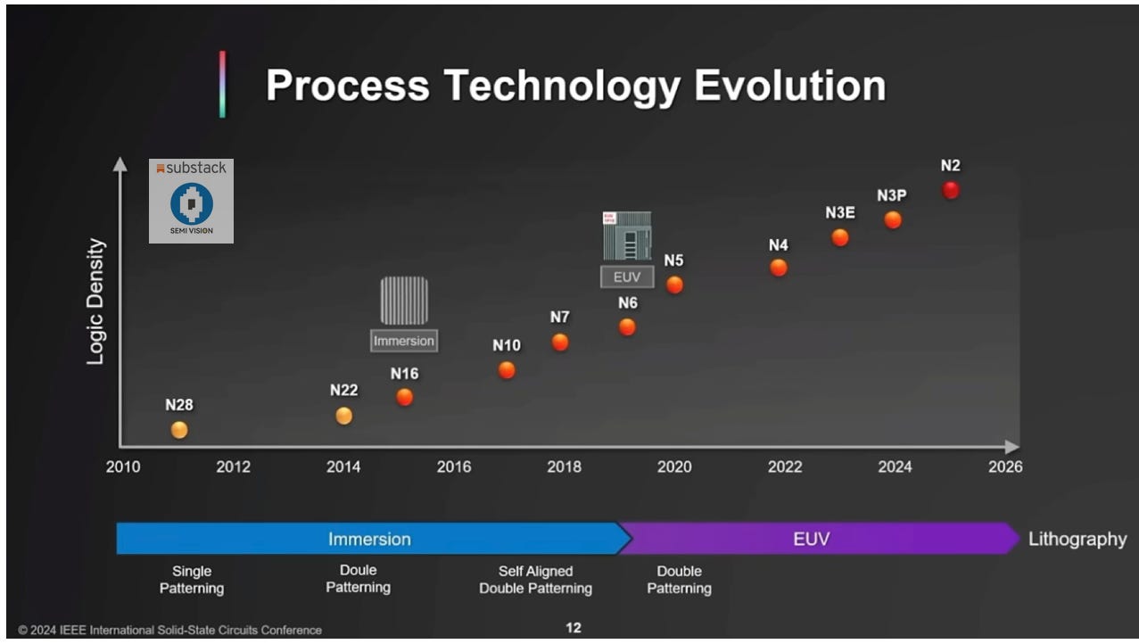
Understanding Advanced Process Technology Evolution — Starting from 4nm Baseline
To better understand advanced logic process technology, it’s helpful to use 4nm (N4) as a baseline node for analysis.
What Does "1P12M" Mean in Process Technology?
At N4, the notation 1P12M refers to the process having 1 Poly layer and 12 Metal layers. This gives a clear indication of the basic mask layers required for 4nm manufacturing.
In logic process development, several important questions need to be addressed, including:
Device characteristics (e.g., VT, Id…)
Spice Model accuracy
WAT (Wafer Acceptance Test) results
CP (Chip probeing) and FT (Final Test)
These fundamental aspects of process development will be covered in detail in a future article series by SemiVision, where we will walk you through how a logic process is developed from scratch, including the challenges encountered at each stage.

Process Comparison: N4 vs Other Nodes
Using N4 as a baseline, SemiVision has also compared different process nodes (N3E, N3B, N2) to highlight their key differences. One critical focus area is the lithography process, especially in terms of the exposure sources used:
EUV (Extreme Ultraviolet Lithography)
ArF Immersion Lithography
ArF Dry Lithography
KrF Lithography
Each of these exposure sources has different intensity and wavelength characteristics, which directly affect exposure accuracy and process window.
To evaluate lithography quality, fabs use two important metrics:
CD (Critical Dimension) – Measuring the exact linewidth printed on the wafer.
AA (Alignment Accuracy) – Evaluating the overlay precision between layers.
Lithography Tools and Foundry Strategies
Different foundries adopt different combinations of lithography tools. However, for EUV processes, the dominant tool supplier is ASML, which provides all of TSMC’s EUV equipment.
According to TSMC’s latest technology forums, process technology evolution can be divided into key stages:
DUV Immersion Lithography (Single Patterning, Double Patterning, and Self-Aligned Double Patterning)
EUV Lithography (first introduced at 7nm)
TSMC’s Mastery of EUV Technology
Starting from 7nm, TSMC gradually incorporated EUV equipment, and has since pushed EUV technology to its limits. This has enabled TSMC to continuously advance logic technology, culminating in the breakthrough development of the A16 process, representing the cutting edge of logic manufacturing technology. In short, lithography technology and mask layers are crucial factors in process evolution, directly affecting cost, yield, and performance. By mastering EUV and combining it with innovative process techniques, TSMC has solidified its leadership in advanced logic technology, creating a strong foundation for future nodes like A16 and beyond.
Stay tuned for SemiVision’s upcoming deep-dive series on logic process development, where we will cover the complete journey from initial development to mass production, including the key challenges and technical breakthroughs along the way.
Related Question:
How Did SMIC Achieve 5nm Process Technology?
Will TSMC Adopt High-NA EUV? At Which Node?
What is Intel’s Progress on High-NA EUV?
What is ASML’s High-NA EUV Development Status and Shipment Forecast?
These are all topics that our SemiVision team has thoroughly researched, and we will be sharing detailed insights and analysis in our upcoming articles on Substack
The Rise of Custom AI Chips in the Era of AI Revolution
As artificial intelligence (AI) technology continues to surge, global tech giants are racing to develop their own custom AI chips, aiming to gain a competitive edge in this rapidly evolving industry. Custom AI chips enhance computing efficiency, reduce reliance on third-party suppliers, and optimize cost structures. However, developing AI chips is highly challenging, requiring substantial financial and resource investments.
The Rise of Custom AI Chips
Google has advanced its custom AI chip development to the sixth generation Trillium TPU (Tensor Processing Unit). Google's custom AI chips now dominate over 70% of the ASIC cloud server market.
OpenAI is reportedly secretly developing its own AI processor, planning to submit its chip design to TSMC for 3nm MPW (Multiple Project Wafer) production in the coming months. Mass production is expected by 2026, utilizing TSMC’s A16 process.
Amazon AWS has announced that by 2024, over half of its global new CPU compute power will be based on its custom Arm-based Graviton series chips, reinforcing the trend of cloud service providers shifting toward in-house chip development.
The shift toward custom AI chips is reshaping the cloud computing and AI hardware landscape, as leading companies seek greater performance, efficiency, and control over their AI infrastructure.
Table: Cloud Service Providers’ GPU/ ASIC Status Update

Regarding Google, many are particularly interested in OCS (Optical Circuit Switch). This technology uses MEMS processes to produce mirrors, whose primary function is to reflect light. OCS operates in a matrix array configuration, which significantly improves overall efficiency, power consumption, and the architecture of AI networks.
Furthermore, how to integrate silicon photonics into future AI chip designs is also a critical question. SemiVision team has also prepared a series of articles covering this topic in detail.
TSMC’s A16 Process: A New Architectural Leap with GAA & SPR
TSMC’s A16 process represents a revolutionary shift in semiconductor design, adopting GAA (Gate-All-Around) transistor architecture along with the Super Power Rail (SPR) process. This transition introduces significant challenges for chip designers, as it requires moving the Power Domain from the Front Side to the Backside, marking a major design innovation.

TSMC’s Transformer Mechanism for Node Migration
To facilitate the transition from 3nm (FinFET) to 2nm (GAA), TSMC has developed a transformer mechanism that allows customers to convert their 3nm FinFET GDS designs into GAA-based designs seamlessly. This system reduces learning curves and enhances efficiency, enabling smoother migration between process nodes.
Similarly, moving from 2nm to A16 will present even greater complexities, particularly in handling Power Domain re-architecture. In response, TSMC’s engineering teams are actively developing a transformer solution to streamline the migration process from N2 to A16, ensuring optimal performance and design efficiency for its customers.
TSMC’s 2nm Adoption & MPW Shuttle Demand
To ensure a smooth transition to the 2nm process for its major customers, TSMC has onboarded over 30 customers in its MPW (Multi-Project Wafer) shuttle program. This highlights the fact that certification for this node requires time, but it also confirms the strong market demand for 2nm.
According to SemiVision’s analysis, N3E vs. N2 PPA (Performance, Power, and Area) comparison demonstrates significant advantages, reinforcing the strong demand for N2 adoption.

Key PPA Metrics to Evaluate Node Performance
When evaluating process nodes, three key indicators must be considered:
Speed Improvement – Measures performance gains at the same power level.
Power Reduction – Measures efficiency improvements at the same performance level.
Chip Density – Indicates transistor density and overall scaling benefits.
Observing N2 vs. N3E, we can see notable efficiency gains, validating the industry's strong interest in TSMC’s 2nm process. This also explains why TSMC’s Arizona (AZ) fab is planning to adopt 2nm, ensuring global competitiveness and advanced manufacturing capabilities in the U.S..
Broadcom Business: Dominating the ASIC & SerDes Market
Broadcom is a dominant player in the ASIC market, with key customers including Google, Meta, Bytedance, OpenAI, Apple, and Fujitsu. Among them, OpenAI stands out as the most intriguing, as it has adopted
3.5D XDSiP packaging technology—an advanced packaging platform co-developed by Broadcom and TSMC.
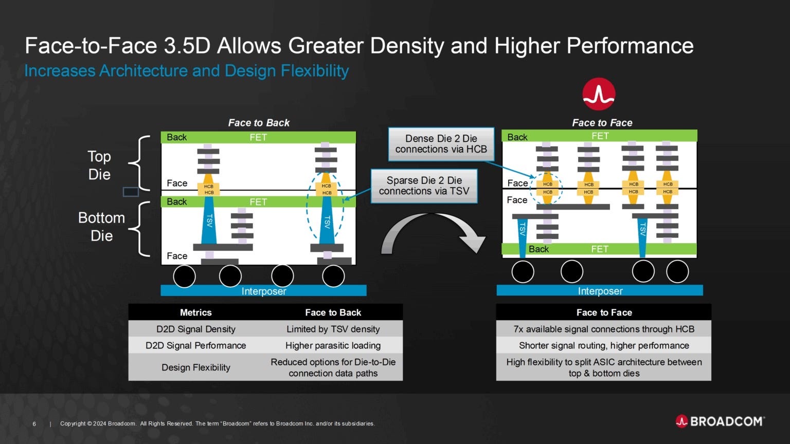
This packaging solution leverages a chiplet architecture with F2F (Face-to-Face) bonding technology, providing significant advantages in the ASIC sector.
Table: Broadcom ASIC Status Update

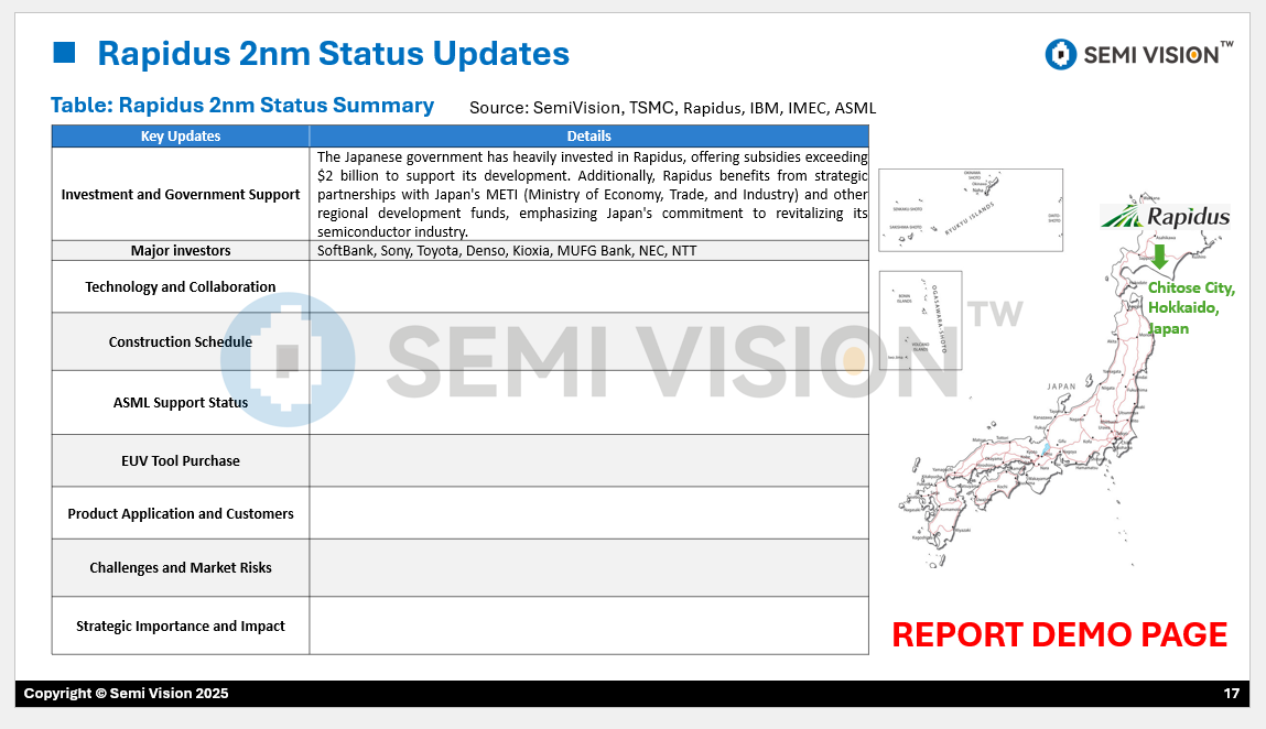
Regarding Broadcom’s ASIC customers, special attention should be given to Fujitsu, as Japan is actively advancing its 2nm process deployment. This includes the establishment of the Rapidus fab in Hokkaido, which will focus exclusively on 2nm production.
According to SemiVision’s research, EUV tool installation at Rapidus has proceeded smoothly, and Broadcom has already joined the Pilot Run process.
It is also worth exploring how Fujitsu plans to leverage the 2nm process for supercomputer manufacturing and its packaging architecture. This is particularly interesting because Rapidus has very limited experience in logic manufacturing, skipping conventional learning curves and directly entering 2nm GAA FinFET technology.
This reflects Japan’s ambition to revive its semiconductor industry after the "lost 30 years," particularly by riding the AI wave. However, it’s important to remember that Japan remains a critical supplier of semiconductor equipment and materials, playing an indispensable role in the global semiconductor ecosystem.
Finally, the SemiVision team has conducted in-depth research into Rapidus, and we will share our findings in future reports.
Marvell Business: A Giant in SerDes & Optical Interconnects
Marvell specializes in SerDes, Optical DSP, PCIe, and Datacenter Interconnect Optical Modules.
SerDes is a critical interface technology, with 224G as the current development focus.
Major suppliers in this domain include Broadcom, Marvell, and MediaTek (MTK).
Looking ahead, Marvell has a strong position in transitioning from 224G to 448G SerDes, giving it a competitive edge in future high-speed interconnects.
Marvell & AWS Collaboration: A Complex ASIC Partnership
Marvell has a strategic partnership with AWS and AIchip, involving a complex collaboration in ASIC development. The ASIC tapeout process must consider:
IP Integration
Front-End Design
Back-End Design
Packaging Design
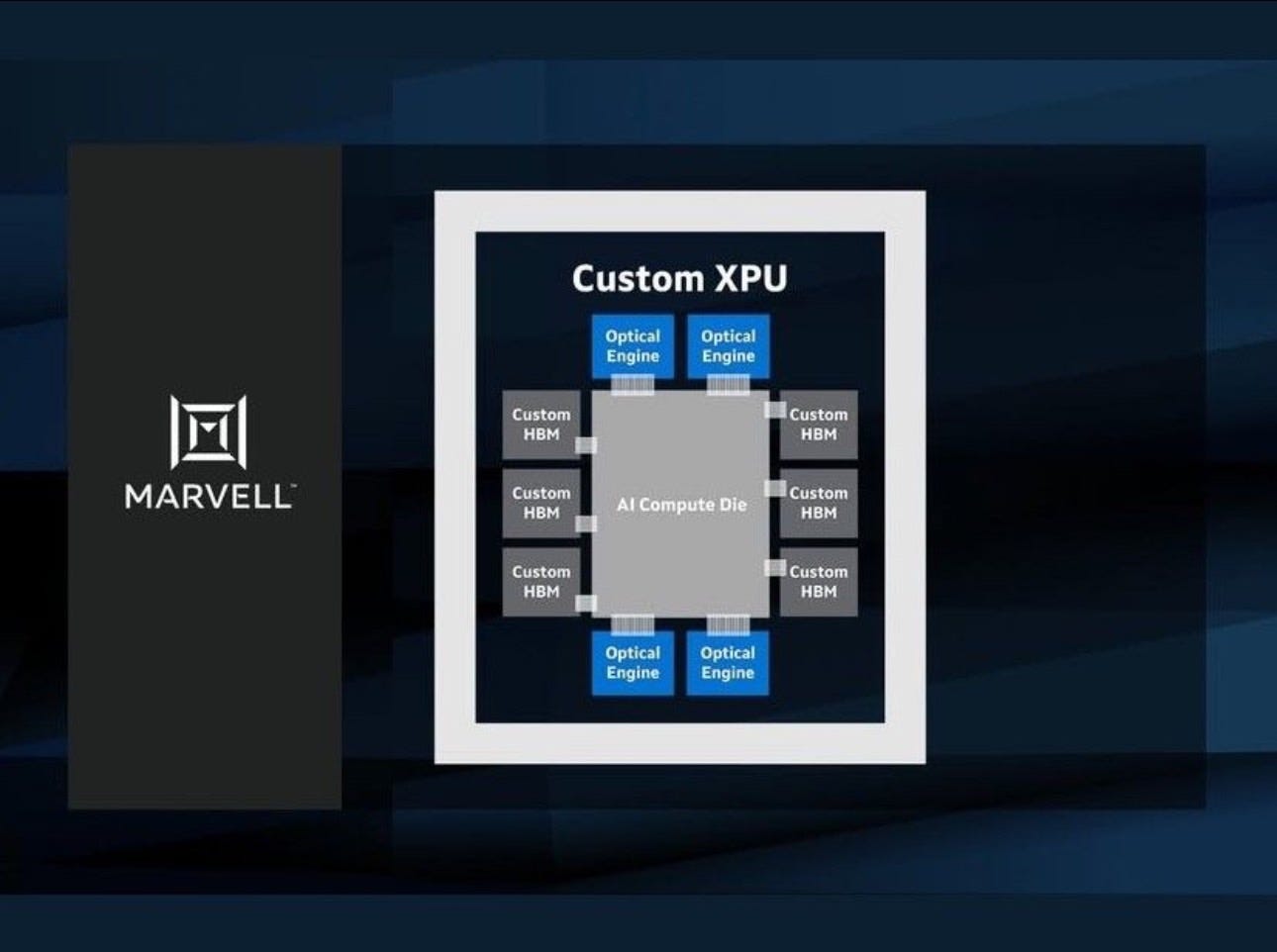
Marvell: Advancements in Advanced Packaging Technologies
One key aspect to watch is advanced packaging, where both Marvell and AIchip have developed their own proprietary packaging technologies. Marvell has integrated Optical Engine technology into its advanced packaging platform, incorporating:
Chiplet architecture
D2D (Die-to-Die) interconnect technology
High-speed optical communication integration
This approach enhances performance, scalability, and power efficiency, making Marvell a strong player in next-generation ASICs.
AIchip’s Custom Advanced Packaging
Alchip Technologies is a founding member of TSMC’s OIP 3DFabric™ Alliance by using the TSMC 3nm process technology and advanced packaging capabilities. Similarly, AIchip has also developed its own advanced packaging solutions, leveraging chiplet-based integration and optimized interconnect technologies. This allows AIchip to compete in the high-performance computing (HPC) and AI accelerator market.
As advanced packaging becomes a crucial differentiator in the AI and data center industry, both Marvell and AIchip’s innovations will shape the future of high-speed, power-efficient computing architectures.

Table: Marvell vs. Alchip: Partnership Roles in AWS’s Trainium 3 Development

Table: AWS Products’ Feature Comparison

Regarding ASIC AI chip design nodes, the focus is primarily on 7nm, 4nm, and 3nm, with future development extending to 2nm and 1.6nm. These nodes represent the current and future process technologies offered by TSMC to its customers. One notable player to watch is SMIC, as SMIC’s Ascend chip has become a crucial product for China’s AI chip development efforts.
As the AI chip race intensifies, monitoring both leading-edge nodes and geopolitical shifts will be critical for understanding the future competitive landscape.
Table: AI ASIC Leading Companies Summary

Global Players in AI ASIC Chips: US, Taiwan, Japan, and China
In the AI ASIC chip race, key players are emerging across different regions:
US players: Marvell, Broadcom
Taiwan players: AIchip, GUC, MediaTek (MTK)
Japan players: Socionext
EU Players: ARM
China’s Push for In-House AI Chips
China is aggressively developing its own AI chips, with a strong focus on the Ascend series from Huawei. Notably, the Ascend 910A is reportedly based on existing chip inventory, reflecting the impact of export restrictions.
The SemiVision team has conducted a comprehensive performance comparison between Huawei’s Ascend 910 series and several mainstream AI chips, including:
Nvidia H100 / AMD MI300X / Nvidia A10 / Google TPU v5 / Nvidia L40S / Google TPU v4 / Nvidia H20 / Huawei Ascend 910B
SemiVision’s Competitive Analysis

The analysis clearly shows that Ascend 910 delivers competitive performance, making it a viable AI accelerator in China’s ecosystem. However, to ensure future supply and performance scaling, SMIC is actively building out its 5nm (N+3) process capability, specifically to support advanced AI chip production.
China’s combination of in-house chip design (Ascend) and domestic foundry capacity (SMIC) highlights its determined strategy to reduce reliance on foreign technology while accelerating its AI ambitions.
The shipment forecast of Huawei’s AI Accelerators (Unit)

The High Cost of AI Chip Development
Developing AI chips comes with enormous financial challenges. NVIDIA CEO Jensen Huang revealed that the latest generation of AI GPUs required an R&D investment of up to $10 billion, with each chip costing between $30,000 to $40,000.
Additionally, running large-scale AI models like ChatGPT is also highly expensive, with each query costing approximately $0.04.
As a result, companies considering in-house AI chip development must carefully evaluate the balance between R&D costs and expected returns.
Balancing Innovation and Cost in AI Chip Development
While custom AI chips have become a strategic necessity for tech giants seeking a competitive edge, the high cost of development poses a major challenge.
To succeed in the AI race, companies must strike a balance between innovation and cost efficiency, ensuring that their custom silicon investments drive both technological advancements and sustainable business growth.
The Impact of DeepSeek on ASIC Development
DeepSeek’s open-source model and relatively low training costs may encourage more companies to develop their own ASIC chips. At the same time, different companies have their own strategies and progress in ASIC design and applications. However, due to DeepSeek’s open-source ecosystem, compared to other AI platforms, DeepSeek’s openness has led to significant changes in the AI field.

DeepSeek’s Technology and Applications
Currently, DeepSeek is widely applied on both mobile and platform ends, even integrated into WeChat, with tens of millions of daily active users. This large-scale user engagement allows DeepSeek to rapidly improve as it benefits from extensive training data and debugging.
ASIC Trends
Many major cloud service providers (CSPs) are now looking to develop their own GPUs and AI chips, not just for training but also for inference. This has fueled a wave of in-house ASIC development, as companies seek to optimize performance and efficiency in AI workloads.
Paid Subscribers Area will provide extra table of
Table: Cloud Service Providers’ GPU/ ASIC Status Update
Table: Broadcom ASIC Status Update
Table: Marvell vs. Alchip: Partnership Roles in AWS’s Trainium 3 Development
Table: AI ASIC Leading Companies Summary
Table: AWS Products’ Feature Comparison
If you are interested in the blank part of information, feel free to contact us via email: jett@semivisiontw.com or refer to our report.