


How TSMC’s Silicon Photonics Could Impact NVIDIA’s Future
Original Article by SemiVision Research


Before reading this article, we recommend referring to SemiVision Research previous coverage on NVIDIA’s silicon photonics and Co-Packaged Optics (CPO) for additional context.
2025 GTC Review: The Silicon Photonics Era Has Arrived – Get Ready!
2025 Nvidia GTC Preview: Insights into Nvidia’s AI Ecosystem
Nvidia GTC AI Conference Preview: GB300, CPO switches, and NVL288
TSMC and NVIDIA Pioneering the Future of AI with Silicon Photonics Technology
CPO Switch Technology Analysis
How to Distinguish Between CPO and OIO? What Is Their Fundamental Difference?
TSMC’s Silicon Photonics Developments and Implications for NVIDIA
To understand NVIDIA’s direction in silicon photonics, we must first analyze TSMC’s progress in this field. The reason is straightforward—NVIDIA is actively collaborating with TSMC. As a semiconductor giant, TSMC’s broad range of process nodes allows it to leverage mature processes for PIC (Photonic Integrated Circuit) manufacturing.
2025 GTC Review: The Silicon Photonics Era Has Arrived – Get Ready!
Benefit of Silicon Photonics
SemiVision Research has prepared a keynote introduction about silicon photonics, which we will soon share exclusively with our subscribed members. Here’s a brief summary:

Traditional data transmission methods, such as copper interconnections, are typically high-speed and optimal for short-distance communication. However, as transmission distances increase, power consumption significantly rises. This makes copper interconnections primarily suitable for inter-chip, on-board, and backplane applications.
Optical transmission, however, exhibits much lower losses over longer distances compared to electrical transmission, making it ideal for extended-range communications. Although optical transmission typically uses a single channel per fiber, leveraging the wave properties of light, silicon photonics can employ wavelength-division multiplexing (WDM) to divide a single optical channel into multiple wavelengths (channels), wavelength channel 1, wavelength channel 2 and further.
Each wavelength can carry a specific bandwidth, meaning the greater the number of wavelengths, the larger the overall bandwidth becomes.

As a result, silicon photonics has become increasingly important due to its high reliability—achieved through semiconductor manufacturing processes—as well as its low power consumption. The realization of silicon photonics, however, heavily depends on foundry capabilities. Ultimately, it requires the integration of photonic integrated circuits (PICs) with electronic integrated circuits (EICs) through advanced packaging techniques, forming what is known as an “optical engine.”

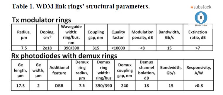
According to SemiVision Research, PIC fabrication requires around 30+ mask layers, with key components including waveguides, GePD (Germanium Photodetectors), and modulators. Modulators adjust optical properties, and their fabrication involves ion implantation, requiring specific masks.
Key Findings from TSMC’s IEDM 2024 Research on Silicon Photonics


High-Performance Silicon Photonics Platform for Next-Gen Data Communications
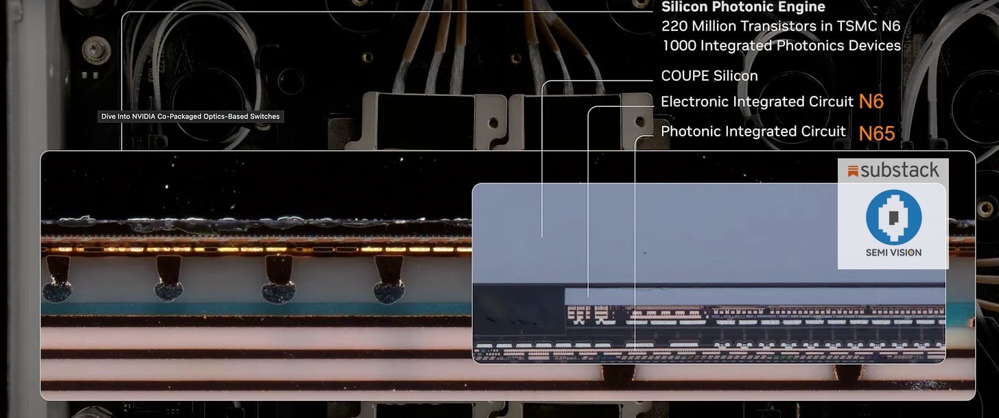
TSMC has developed an advanced silicon photonics foundry platform using 300mm wafer processing, integrating PIC (N65 and beyond) and EIC (N7 and beyond) process nodes.

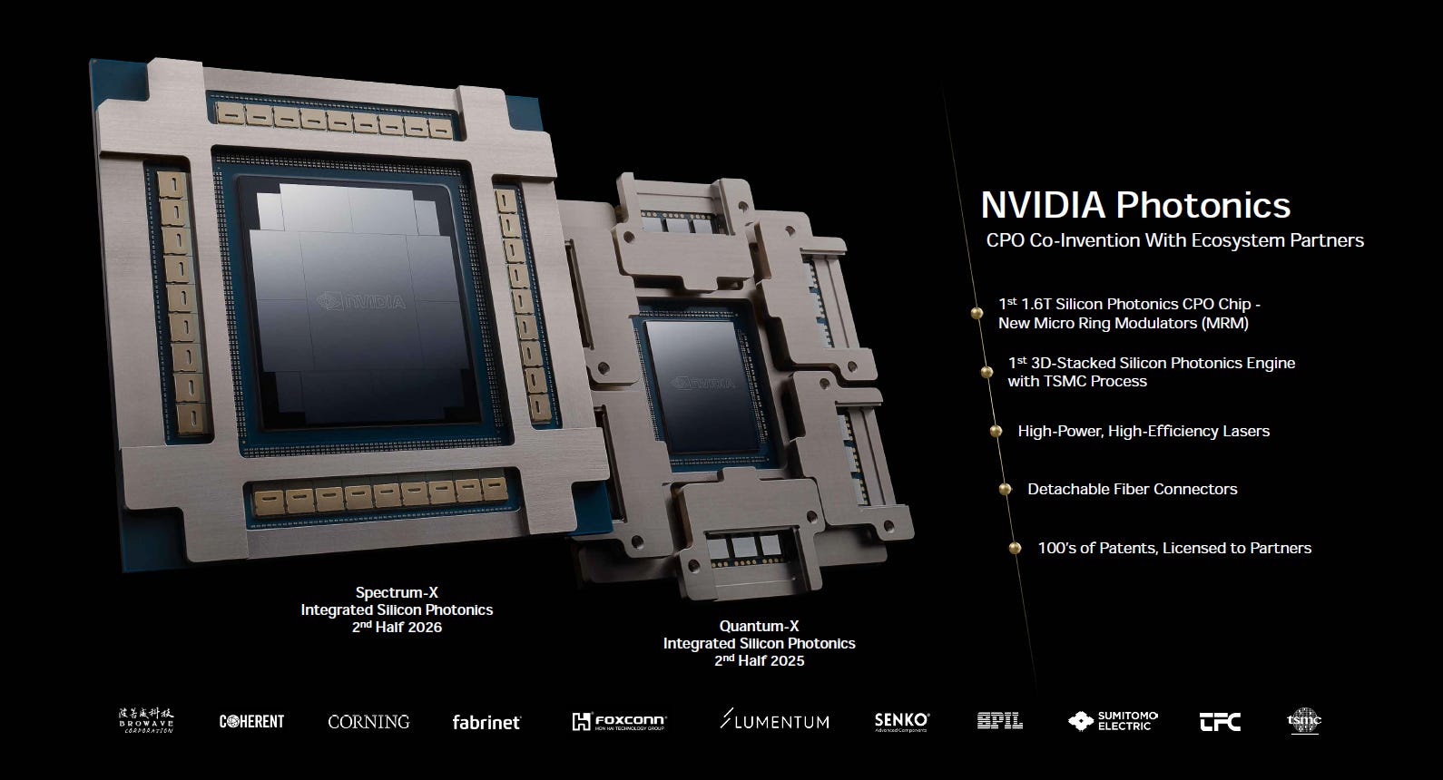
2025 Nvidia GTC , they proposed the silicon photonic solution:
• ASIC (Quantum X800) adopts the N4 (4nm) process
• EIC (Electronic Integrated Circuit) adopts the N6 (6nm) process
• PIC (Photonic Integrated Circuit) is still mainly based on the N65 (65nm) process
This combination reflects Nvidia’s design considerations:
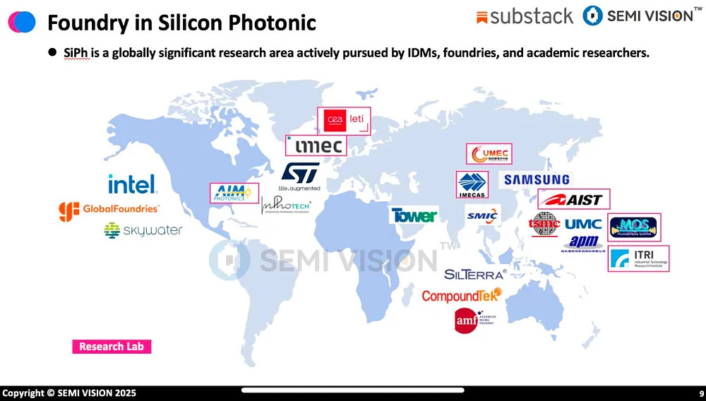
Silicon Photonics is a crucial driver for AI chips. Currently, since silicon photonics mainly relies on wafer fabs for production, the Semivision team has compiled a list of global wafer fabs and research institutions involved in silicon photonics chip manufacturing.
It is evident that Taiwan, including TSMC and UMC, possesses this capability. Notably, TSMC not only has a silicon photonics platform, COUPE, but also the ability to integrate Optical Engine(OE) with advanced packaging. As a result, Taiwan plays a vital role in driving the silicon photonics industry forward.
1. High-performance computing core (ASIC) uses the more advanced N4 process to enhance performance and energy efficiency.

2. EIC (electronic integrated circuit) opts for theTSMC N6 process, balancing power consumption, cost, and performance.
TSMC currently provides both PIC and EIC manufacturing processes, along with advanced hybrid bonding packaging technology. As we know, an optical engine requires the integration of PIC, EIC, and advanced packaging technologies simultaneously. In addition to TSMC, several other foundries are actively developing similar capabilities. SemiVision Research will provide detailed analysis and explanations regarding global foundries with silicon photonics processes in the future.
3. PIC (photonic integrated circuit) remains on the TSMC N65 process, as photonic components (such as waveguides, modulators, and detectors) do not require aggressive scaling like traditional transistors, and a mature process is sufficient.
This aligns with TSMC’s high-performance silicon photonics (SiPh) platform proposed at IEDM 2024, particularly the N65 + 12-inch process for PIC, ensuring the reliability and manufacturability of silicon photonics technology
Traditional Optical Modules —>CPO Optical Modules
Revolutionizing Networking for the Era of Agentic AI
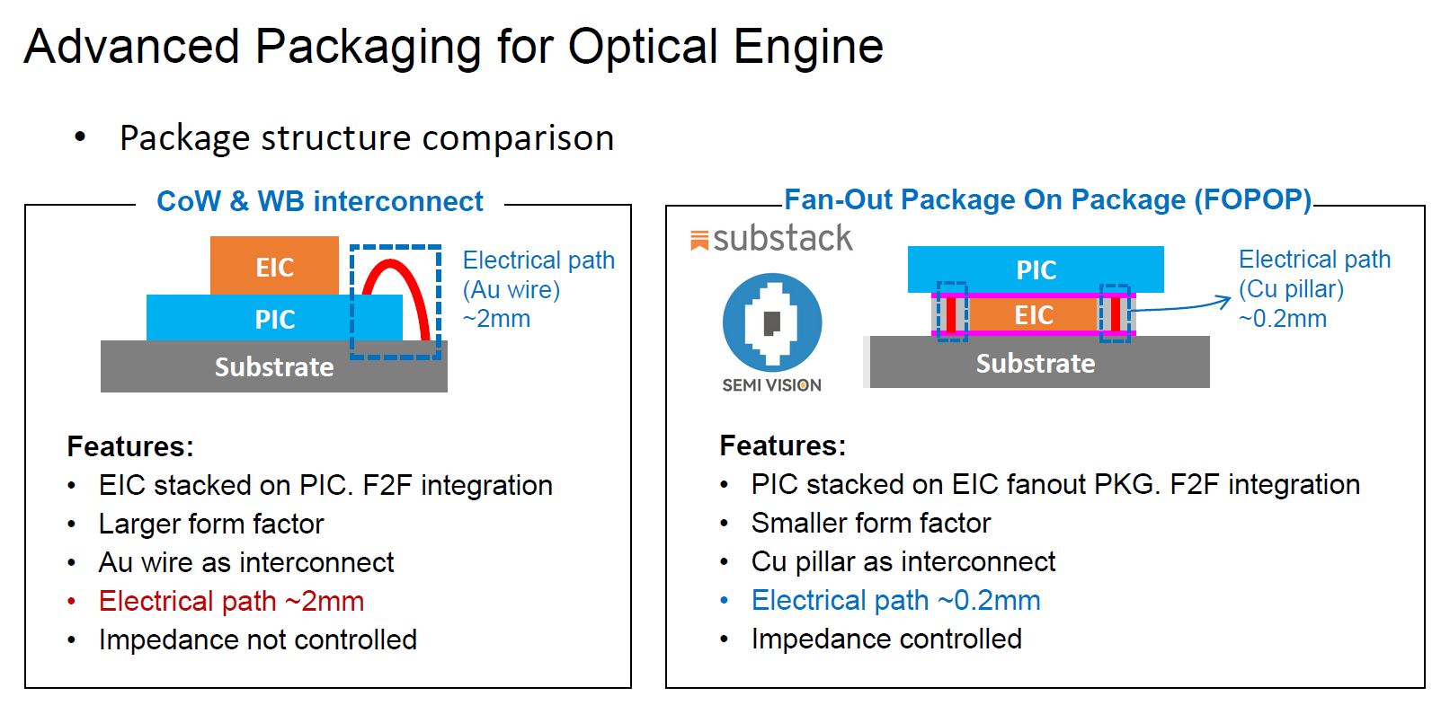
Heterogeneous integration via COUPE or CoWoS
CoWoS enables tight PIC-EIC integration.

TSMC has integrated OE (Optical Engine) with Advanced Packaging, forming what can be referred to as iOIS — an Integrated Optical Interconnection System. However, this platform is specifically focused on optical interconnect applications.

To support the growing demand for silicon photonics, TSMC has introduced a dedicated platform named COUPE, tailored for optical engine integration. This platform is aimed at advancing high-speed, low-power optical interconnects in next-generation systems

SemiVision Research has an in-depth understanding of the CoWoS supply chain. According to current insights, a “local-to-local” trend has begun to emerge within TSMC’s CoWoS supply chain.

CPO Packaging Solution
ASE: Advanced Packaging for Optical Engine
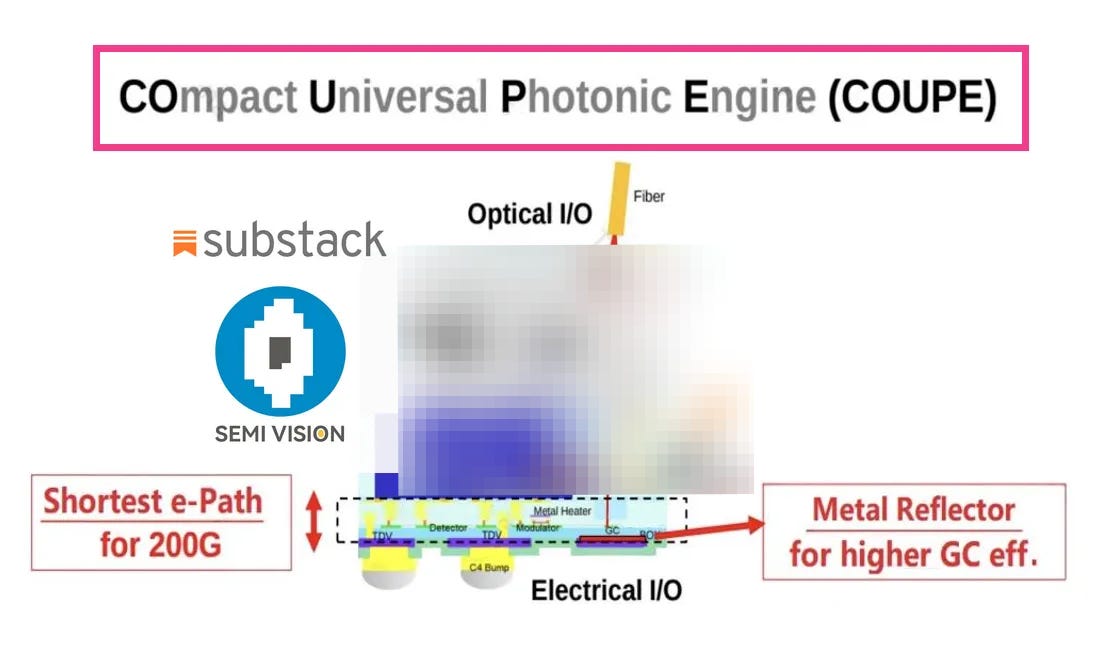
TMSC: COUPE (Compact Universal Photonic Engine) integrates vertical O-band grating couplers (GC) with embedded micro-lenses, achieving 0.3dB fiber-array coupling loss with ±10μm alignment tolerance.

SemiVision Research will conduct in-depth discussions on the following issues in the future.
What’s shortest e-path for 200G?
What’s Metal Reflector for higher GC efficiency ?
What’s function in Metal Heater in PIC?
What’s Support Silicon ?
What’s u-LENS ?
What’s Optical I/O and how to coupler to Fiber?

For Paid Members, SemiVision Research will discuss the following topics:
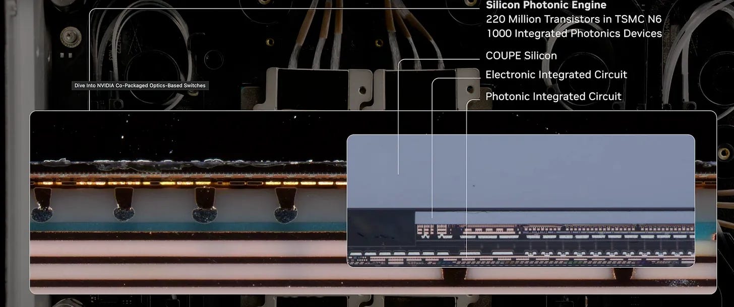
NVIDIA Silicon Photonics Engine (Referred to as “Optical Engine” by TSMC)
CPO Development statute updated (AMD (Ranovus), Broadcom, Cisco, IBM, Intel, and Marvell)
Silicon Photonics Manufacturing Process
CPO Process Flow
Automated Testing & Reliability(PIC + EIC)
Critical Dimension (CD) Uniformity Control
Photolithography to optical device (PIC)
Process Design Kit (PDK) in PIC
Silicon Photonic Application
