

Breaking the AI Interconnect Wall: Strategic Insights from the TSMC × Avicena Optical Alliance
Original Articles By SemiVision Research (TSMC , Nvidia ,Avicena ,NYCU , Foxconn , ITRI )

TSMC × Avicena: A Strategic Alliance Shaping the Future of Optical Interconnects Beyond Display
As generative AI and high-performance computing (HPC) drive exponential demand for bandwidth and energy efficiency in chip-to-chip communication, traditional copper interconnects are approaching their physical limits. These legacy interconnects can no longer meet the growing needs for low latency, high density, and ultra-low power in next-generation system architectures.

In response to this I/O revolution, TSMC has announced a strategic partnership with U.S.-based optical interconnect startup Avicena, focused on developing microLED-based chip-to-chip optical communication technologies.
This collaboration marks TSMC’s official entry into the use of Micro LED beyond display applications, opening a new dimension for advanced packaging and photonic-electronic co-design. By combining Avicena’s innovative LightBundle microLED optical engine with TSMC’s industry-leading advanced integration platforms — including SoIC, InFO, and CoWoS — the two companies are charting a bold path from the limitations of “copper walls” to a future defined by “light walls.”
This partnership is more than just a technological convergence — it represents a fundamental redefinition of how chips communicate in the era of disaggregated and optical computing.
Taiwan’s Momentum in C2C Optical Interconnects: Industry and Academia Unite
Taiwan is rapidly emerging as a critical hub in the evolution of chip-to-chip (C2C) optical interconnects, driven by dynamic collaborations between academia and industry:
Foxconn Research Institute (鴻海研究院) has partnered with National Taiwan University and King Abdullah University of Science and Technology (KAUST) to present breakthrough multi-wavelength μLED technology at CLEO 2025. This achievement, enabling high-speed visible-light chip-to-chip communication, marks a significant advance toward commercial optical interconnect platforms .

Leading academic groups, including Prof. Ho-Chung Kuo (郭浩中) from National Yang Ming Chiao Tung University, have published extensively on GaN μLEDs and their integration with silicon photonics—highlighting Taiwan’s deep bench in fundamental and applied R&D.

Professor Jui-Hwa Hung(洪瑞華): A Pioneer in Next-Generation Power and
In the rapidly evolving landscape of Taiwan’s semiconductor and optoelectronic industries, Professor Jui-Hwa Hung stands as a pivotal figure. Currently serving as a Chair Professor at the Institute of Electronics, National Yang Ming Chiao Tung University (NYCU), Professor Hung has long dedicated her research to epitaxial thin-film transfer, wide bandgap semiconductor device engineering, and micro-scale optoelectronic integration. Her contributions have helped lay the foundation for Taiwan’s advancement in high-frequency, high-temperature, and high-efficiency device technologies.

Academic Excellence and Global Perspective
Professor Hung earned her undergraduate degree in electrical engineering from National Cheng Kung University and her Ph.D. in electrical engineering from National Sun Yat-sen University. She has held leadership roles across academic institutions, including as Department Chair at NYCU and Dean of the College of Engineering at National Chung Hsing University. Her research group, the Advanced Semiconductor Process and Device Laboratory, has specialized in heteroepitaxy, microstructure transfer, and novel optoelectronic device fabrication.
Innovation in Wide Bandgap Semiconductor Research
Amid the global transition from Si and GaN to ultra-wide bandgap materials like β-Ga₂O₃, Professor Hung has been at the forefront of this movement in Taiwan. Her research team has achieved significant breakthroughs in integrating β-Ga₂O₃ on silicon and sapphire substrates, addressing key challenges in heteroepitaxy and high-voltage device architecture. Her work has been recognized with prestigious awards, including the Ministry of Science and Technology’s Outstanding Research Award.
Bridging Academia and Industry: From Lab to Fab
Professor Hung actively collaborates with major research institutes such as ITRI and the Foxconn Research Institute, aiming to translate academic research into commercial-scale technologies. In the field of microLEDs, her team has successfully developed GaN-on-sapphire μLED arrays compatible with CMOS processes, exploring their application in chip-to-chip optical interconnects (C2C Optical I/O). She is among the first in Taiwan to integrate μLED technologies with advanced packaging platforms like TSMC’s SoIC and CoWoS for next-generation optical communication modules.
She also frequently collaborates with her husband, Professor Tung-Hsing Wu, a fellow expert in optoelectronics. Together, they are known as a “power couple” in Taiwan’s academic circles, pushing the boundaries of LED efficiency, packaging, and heterointegration research.
Looking Forward: Driving Heterogeneous Integration with Silicon Photonics
As the semiconductor industry shifts toward chiplet architectures, silicon photonics, and electrical-optical convergence, Professor Hung is leading efforts to merge μLED technologies with photonic platforms. Her research aims to realize highly scalable, thermally resilient, and integration-friendly solutions for data centers, smart vehicles, and edge AI devices.
In an era where traditional copper interconnects and electrical I/O are approaching their limits, Professor Hung offers not just technical innovation but a visionary pathway for how Taiwan can shape the global future of heterogeneous integration.
Her work exemplifies how deep materials science and forward-thinking system design can come together to drive breakthroughs in computing, communication, and intelligent infrastructure.
The Industrial Technology Research Institute (ITRI) actively champions μLED integration into silicon photonic platforms, accelerating technology transfer from lab to fab, and reinforcing Taiwan’s position in the global optical interconnect value chain.

ITRI Leading Taiwan’s Charge in μLED-Silicon Photonics Integration: From Advanced Manufacturing to Electro-Optical Convergence
As generative AI, high-bandwidth transmission, and edge intelligence continue to drive system innovation, silicon photonics is rapidly emerging as a key enabler for next-generation data connectivity and electro-optical integration. In this transformative wave, Taiwan’s Industrial Technology Research Institute (ITRI) has taken on a pivotal role—bridging advanced packaging, photonic device development, and heterogeneous integration. Particularly, its work in merging micro-LED (μLED) with silicon photonics (SiPh) has become a cornerstone of Taiwan’s competitiveness in next-gen optical interconnects.
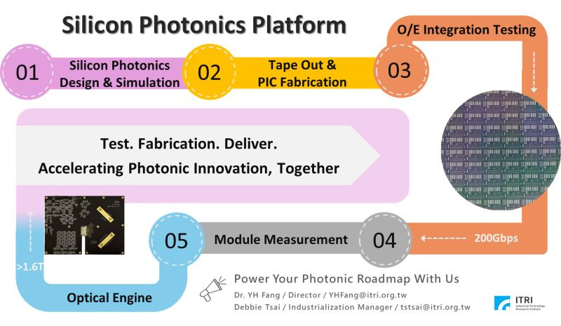
Comprehensive Silicon Photonics Platform Development
ITRI has been deeply engaged in building high-speed optical transceiver modules, including modulators, photodetectors (PDs), and waveguides. Their platform supports data rates exceeding 200 Gb/s per channel and is aligned with future needs such as Co-Packaged Optics (CPO) and Optical I/O (OIO). Leveraging III-V compound integration with CMOS-compatible processes, ITRI has established end-to-end capabilities from design to manufacturing and testing—positioning Taiwan as a global player in the silicon photonics supply chain.
μLED as a High-Speed Optical Source: A Cross-Domain Expansion
While ITRI initially focused μLED technology on high-resolution display applications (e.g., wearable AR, in-vehicle displays), the institute has since expanded its scope. With strong expertise in epitaxial growth, laser lift-off (LLO), micro-transfer, and hybrid packaging, ITRI is now exploring the use of μLEDs as high-speed, low-power optical sources for chip-to-chip and board-level optical interconnects. Their μLED-on-CMOS integration path opens the door to compact, efficient LightBundle-like architectures.
Organizational Teams and Ecosystem Alliances
The core of this R&D effort is led by the Electronic and Optoelectronic System Laboratories (EOSL) within ITRI. EOSL not only drives internal innovation but also collaborates with international partners such as the UK’s CSA Catapult to co-develop platforms tailored for advanced optical packaging—including InFO-Opto and CPO systems.
In parallel, ITRI initiated the “Micro-LED Industry Alliance” in 2016, bringing together over 50 companies across the material, equipment, and component sectors. This alliance strengthens the domestic ecosystem and accelerates the path to commercialization of μLED-based optical modules.
Global Collaboration and Industrial Readiness
ITRI has also actively participated in joint research programs with the U.S., Germany, and the UK to drive cross-border standards and platform convergence. Its μLED and SiPh modules are now available to leading semiconductor fabs such as TSMC and UMC, as well as packaging and system vendors, enabling co-development projects that transition lab-scale technology to high-volume manufacturing.
Taiwan’s Strategic Position in Optical Interconnect Innovation
ITRI’s deep expertise in epitaxy, photonics, precision packaging, and IC integration has positioned Taiwan as a key innovator in the μLED × silicon photonics domain. As the global industry faces bottlenecks in copper-based interconnects and SerDes-limited bandwidth, ITRI’s work lays the technical and manufacturing foundation for Taiwan to lead in data center, AI accelerator, smart vehicle, and edge intelligence applications.
Looking forward, ITRI is expected to remain a cornerstone in Taiwan’s efforts to advance electro-optical fusion, with μLED-SiPh platforms at the heart of the next computing and connectivity revolution.

What Sets Taiwan Apart
Talent Fusion
Taiwan combines world-class researchers like Professor Kuo—a specialist in both GaN μLEDs and silicon photonics—with engineers capable of bridging optical R&D and practical CMOS manufacturing.
Industry – Academia – Government Synergy
Collaborative platforms like Hon Hai Institute and ITRI effectively integrate academic innovation with industrial process capabilities, fostering accelerated innovation cycles.
Manufacturing Readiness
With strong upstream GaN μLED expertise, CMOS process alignment, and packaging infrastructure—including TSMC, UMC, and Samsung—Taiwan is positioned to transform lab prototypes into scalable optical interconnect modules.
Taiwan’s convergence of academic excellence, corporate research, and manufacturing infrastructure, combined with supporting R&D entities like ITRI, provides a robust ecosystem to support the rapid commercialization of μLED-based chiplet communication. This puts Taiwan at the forefront of the global optical interconnect transition and complements cross-border partnerships like TSMC × Avicena.
Why You Absolutely Must Know Avicena !!

1. MicroLED-Based Optical Interconnect Pioneer
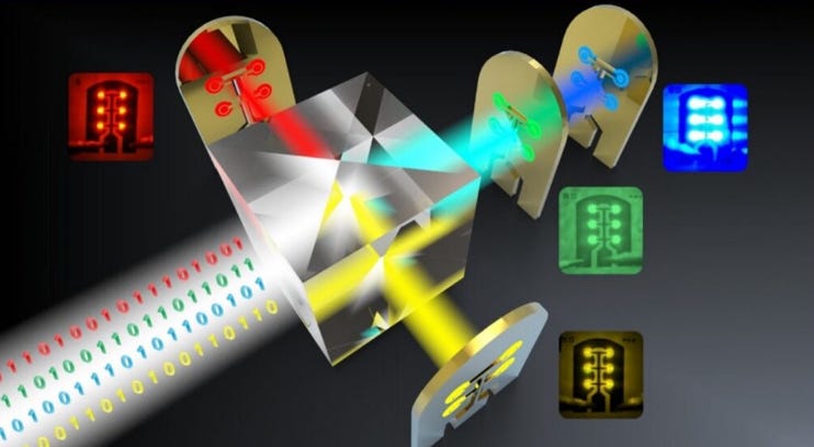
Avicena leads the charge in microLED-based chip-to-chip optical interconnects—a fundamentally different approach from conventional silicon photonics or laser-based solutions .
2. Sub‑pJ/bit Energy Efficiency
Their LightBundle™ platform delivers < 1 pJ/bit—about 5× more efficient than competing optical systems and orders of magnitude better than traditional electrical links, while scaling beyond 10 m for multi-rack GPU clusters .
3. Multi-Tbps/mm² Bandwidth Density
Avicena achieves >1 Tbps/mm² today, with a roadmap toward 10 Tbps/mm²—far outperforming existing optical and electrical interconnect densities .
4. Seamless CMOS & Packaging Integration
Their modular chiplet design supports standard packaging technologies—including CPO, OBO, AOC—and fuses microLEDs + PD arrays into CMOS ICs, enabling integration with UCIe, BOW, and TSMC processes .
5. Funding and Industry Momentum
With US $65M in Series B funding (Tiger Global, SK hynix, Lam Research, others), and partnerships with TSMC and ams OSRAM, Avicena is transitioning from lab to production .
6. Strategic Alliance with TSMC
TSMC’s entry into microLED optical interconnects—via their investment in Avicena—underscores the technology’s high strategic value and accelerates its ecosystem development .
Avicena is spearheading the transition from copper and laser optics to chip-scale microLED optical links, unlocking sub‑pJ/bit efficiency, multi-Tbps/mm² density, and system-level scalability that foundationally reshape AI, HPC, memory, automotive, and edge architectures.
Overview of Core Research Directions at Foxconn Research Institute
1. MicroLED and Silicon Photonics-Based Chip-to-Chip Optical Interconnects (C2C Optical Interconnect)
Foxconn Research Institute is actively developing chip-to-chip optical interconnects based on microLED (μLED) arrays, integrating them with silicon photonics platforms. Collaborating with institutions like National Taiwan University and KAUST, the team focuses on visible light communication (VLC) and compact μLED driver circuits to enable next-generation AI chip packaging and interconnect architectures.
2. Artificial Intelligence and Large Language Model Development (FoxBrain)
The institute has developed its own large language model, FoxBrain, optimized for Traditional Chinese. Trained on 120 NVIDIA H100 GPUs within just four weeks, the model is tailored for applications in smart manufacturing, autonomous driving platforms, and intelligent decision-making systems in smart cities.
3. Fourth-Generation Ultra-Wide Bandgap Semiconductor Devices (β-Ga₂O₃ Power Devices)
In partnership with NYCU and UT Austin, Foxconn is developing β-Ga₂O₃-based lateral power FETs featuring high breakdown voltage, strong current output, and excellent thermal performance, targeting electric vehicles, high-frequency power converters, and industrial-grade power modules.
4. Quantum Computing and Information Theory
The institute has established a dedicated Quantum Computing Center focusing on quantum algorithms and quantum error correction. Its recent work on qudit noise-resilient circuits has gained international attention, positioning it as one of Taiwan’s rare contributors to core quantum computing theory.
5. Cybersecurity, AI Robotics, and Digital Twins
Research areas span AI-driven smart manufacturing, edge robotics control, cybersecurity, and digital twin simulation platforms—supporting Foxconn’s global factory automation and AI integration efforts.
Why This Research Matters
Technical Breadth and Depth: From μLED interconnects and AI language models to β-Ga₂O₃ power electronics and quantum algorithms, Foxconn Research Institute tackles fundamental pillars of next-generation computing and communication infrastructure.
Academic-Industry Synergy: The institute maintains strong collaborations with leading institutions such as NTU, NYCU, KAUST, and UT Austin, enabling fast technology translation from research to commercialization.
High Commercialization Potential: All core focus areas are tightly aligned with emerging demands in AI, EVs, datacenter infrastructure, and edge computing over the next 3–5 years.


For Paid Members ,SemiVision will discuss topics on
NVLink vs. Avicena LightBundle: From High-Speed Electrical to the Future of Optical Interconnects
LightBundle: Reconstructing the Future of Optical Interconnect with MicroLED Technology
Tackling the Three Grand Challenges in ICT Interconnect
Ultra-Low Energy Design: Achieving Sub-pJ/bit Efficiency with LightBundle™
Toward Edge, Automotive, and Mobile: Expanding LightBundle’s Deployment Horizons
Enhancing Bandwidth Density: Addressing the FLOPS-to-I/O Imbalance
Building Terabit-Class Bandwidth Modules with High-Channel Parallelism
Miniaturization and Stacking: Maximizing Module Density through Core Size Reduction
Parallel Optical Transmission: Breaking Free from the Bottlenecks of Serial Architectures
System-Level Implications
Breaking Free from SerDes Limitations: Toward Ultra-Low Latency Interconnects
LightBundle’s Approach: Eliminating the SerDes Stack with Native Parallel Optical Interfaces
Core Technology Components and Manufacturing Foundations
Hexagonal Array and High-Density Optical Coupling Architecture
Multicore Fiber Interconnect: High-Density, High-Reliability Communication Backbone
Thermal Stability and Manufacturing Reliability: Ready for Automotive and Industrial Environments
Comprehensive Capability Assessment
Four Key Application Scenarios: Unlocking the Real-World Potential of μLED Optical Interconnects
From the Data Wall to the Light Wall — LightBundle Unlocks the Next Frontier in Chiplet Integration
LightBundle: A Micro-Scale Optical Platform for the Post-SerDes Era
