

Redefining PIC Design: Variability-Aware Workflows for High-Yield Silicon Photonics
Original Articles by SemiVision Research (Foxconn, TSMC, Nvidia, Intel , LDS, Siemens ,Suruga Seiki , Wave Photonic, ficonTEC, Teradyne , Advantest ,FormFactor, Luceda ,Rain Tree Photonic, A*STAR)

Designing modern silicon photonics (SiPh) systems requires not only a deep understanding of physical structures and fabrication processes, but also relies heavily on engineering experience and a well-established design methodology. Only with a high-quality Process Design Kit (PDK) — containing comprehensive device models and verified design rules — can designers avoid critical errors during layout and verification stages, ensuring a successful transition from concept to manufacturing.
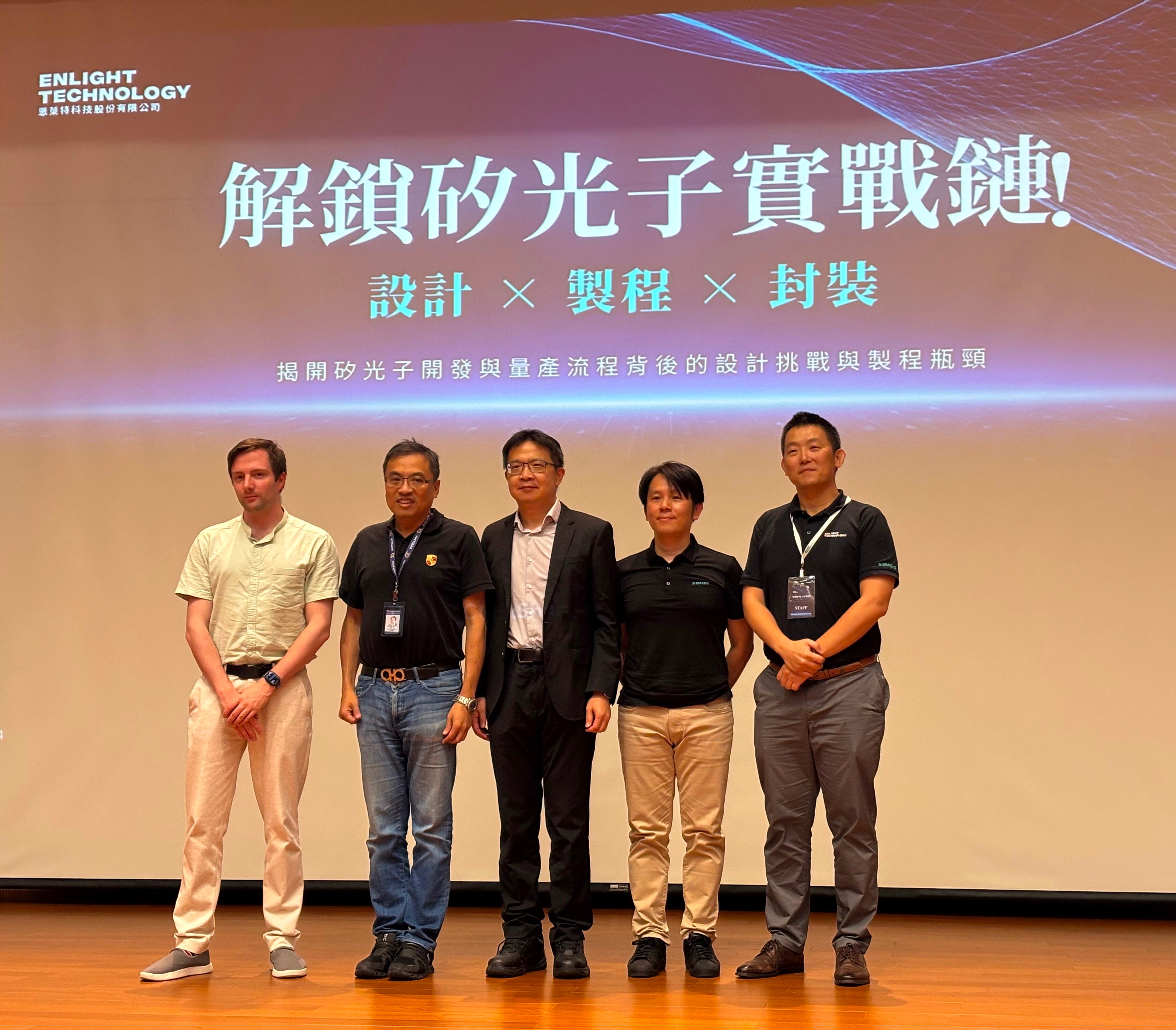
Today, SemiVision participated in the Silicon Photonics Design Seminar hosted by Enlight Technology Inc. (Enlight TEC). The event focused on the practical challenges and future opportunities in silicon photonics design workflows. It brought together leading companies and experts in design, simulation, manufacturing, and optical coupling to share cutting-edge insights and advancements from the front lines of the industry.
Latitude Design Systems
Dr. Terence S.-Y. Chen presented PIC Studio as a comprehensive unified design platform that accelerates end-to-end silicon photonics chip development through deep integration with the foundry ecosystem. His presentation demonstrated how PIC Studio provides a complete workflow spanning from component design and simulation to system-level integration and fabrication-ready verification.
Key highlights of his presentation included the platform's extensive foundry partnerships, supporting both 12-inch silicon photonics foundries and specialized TFLN/SiPh/Compound PDK providers across the industry. Dr. Chen emphasized how this unified approach delivers over 40% cost reduction and 30% faster development cycles compared to traditional multi-tool workflows.
He also showcased the platform's advanced capabilities including the Assembly Design Kit (ADK) integration with PHIX, demonstrating how PIC Studio bridges the gap between photonic design and manufacturing through comprehensive Design Rule Checking (pVerify DRC), advanced schematic-driven layout (SDL), and system-level electro-optical co-simulation capabilities. The presentation highlighted the company's commitment to providing cutting-edge tools that enable customers to bring innovative photonic solutions to market more efficiently.


Siemens EDA

Vincent Lai – Applications Engineer Consultant
Vincent Lai presented Siemens EDA’s strategy for enabling electro-photonic co-design, emphasizing the integration of electronic and photonic design tools into a unified workflow. He highlighted key capabilities such as mixed electro-optical simulation, — essential for validating signal integrity and performance in next-generation PIC designs. Siemens’ approach allows seamless collaboration between photonic and electronic domains, addressing critical needs in AI and high-speed communication systems.
Suruga Seiki Co., Ltd. (Taiwan)

Chris You– Senior Product Marketing Manager
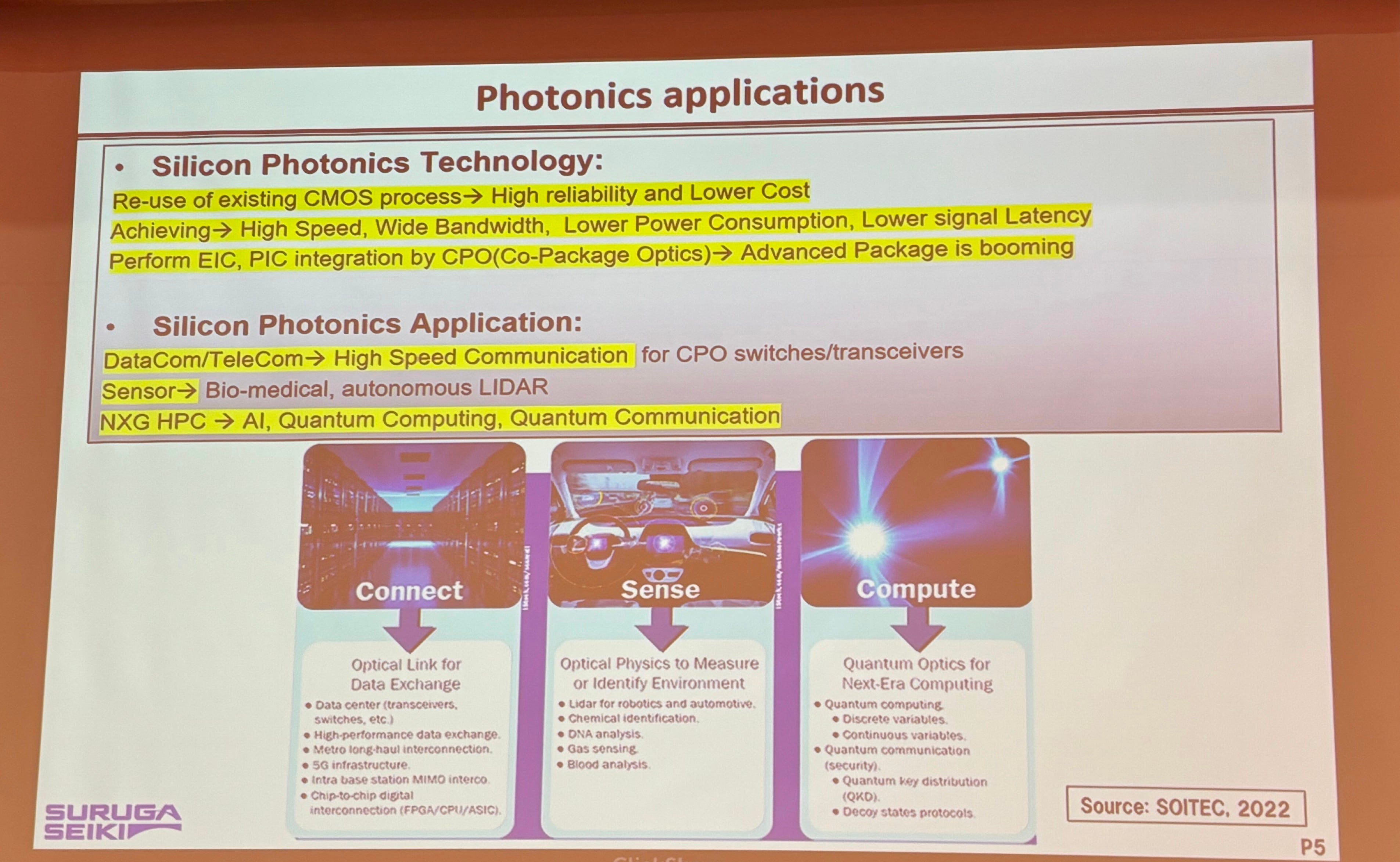
Chris Yu focused on high-precision alignment technologies for FAUs (Fiber Array Units) and their mechanical integration within optical coupling modules. He discussed Suruga Seiki’s expertise in sub-micron positioning systems and alignment stages, which are vital for scalable and reliable optical packaging. His talk also explored the growing relevance of precision opto-mechanics in Co-Packaged Optics (CPO) and Optical I/O (OIO) applications, particularly in AI-driven datacenter environments where efficient optical interfacing is critical.
Wave Photonics
James Lee – CEO & Co-Founder
James Lee delivered an in-depth look at Wave Photonics’ efforts in developing automated photonic design systems capable of spanning multiple material platforms and process nodes. He showcased how their tools support scalable design across silicon, InP, and SiN technologies, enabling robust deployment for 400G/800G transceivers and AI interconnect modules. He also shared insights from Wave Photonics’ participation in international R&D collaborations, highlighting practical lessons from real-world deployments in high-speed optical communications.


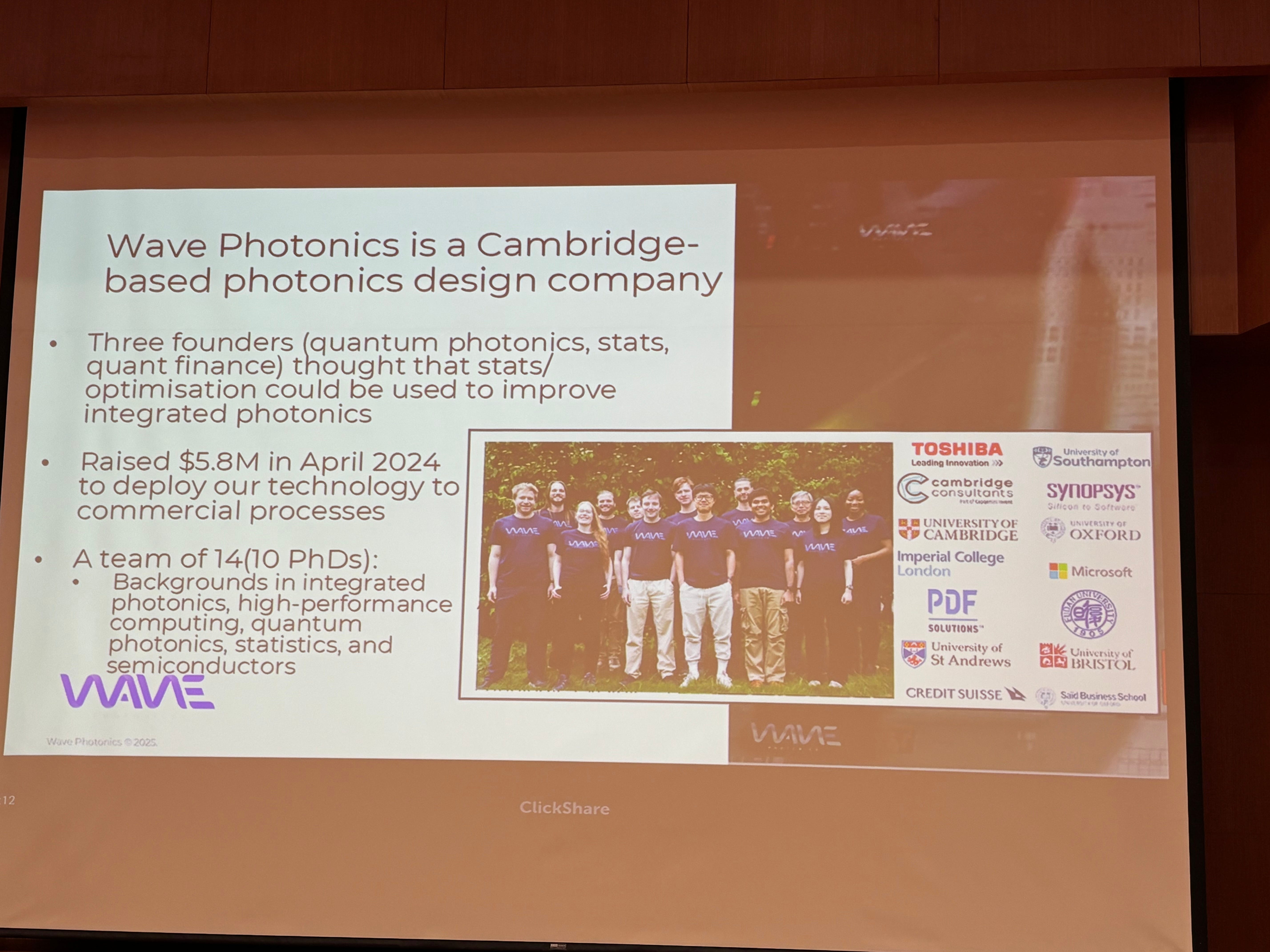
Company Overview: Wave Photonics
Founded in 2021 and headquartered in Cambridge, United Kingdom, Wave Photonics is a deep-tech startup specializing in automated photonic design and process variation management for photonic integrated circuits (PICs).
Core Technology:
The company focuses on developing advanced Process Design Kits (PDKs), featuring over 1,000 components across 33 wavelengths ranging from 493 nm to 1550 nm, with a strong emphasis on quantum applications.
Process Variation Management and Automated Design Workflow
Process Characterization and Modeling:
Wave Photonics utilizes Scanning Electron Microscope (SEM) imaging to characterize fabrication-induced variations. These measurements are used to build high-fidelity fabrication models that capture both the expected average outcomes and multi-dimensional variation profiles.
Automated Design and Optimization:
With its automated workflow, Wave Photonics is capable of developing and re-optimizing entire PDKs in just a few weeks. This dramatically reduces optical losses and improves overall process yield by accounting for real-world variation early in the design cycle.
Tool and Platform Compatibility
Design Tool Compatibility:
Wave Photonics’ PDKs are compatible with multiple industry-standard design platforms, including GDSFactory, Siemens L-Edit, and Cadence Virtuoso. Support for Luceda’s IPKISS platform is also underway.
Packaging and Test Integration:
The company offers QPICPAC packaging services and collaborates with PHIX for component-level characterization, delivering an end-to-end solution from design through packaging.
This seminar not only showcased Taiwan’s growing technical depth in heterogeneous photonic-electronic integration but also highlighted the cross-disciplinary value generated through the convergence of design tools, manufacturing precision, and packaging co-optimization. SemiVision will continue to follow developments in this field closely and actively collaborate with partners across the silicon photonics ecosystem to drive innovation and practical deployment.
At today’s Silicon Photonics Design Seminar hosted by Enlight Technology Inc., the opening keynote was delivered by Prof. Hao-Chung Kuo, Chair Professor at the Department of Photonics, National Yang Ming Chiao Tung University, and Director of the Semiconductor Research Institute at Foxconn Research Institute. A globally recognized expert in silicon photonics, Prof. Kuo opened with a powerful message:
“Driven by the demands of AI and high-speed data transmission, silicon photonics is rapidly transitioning from academic research to commercial applications — and is fundamentally reshaping the semiconductor landscape.”
Prof. Kuo emphasized that silicon photonics is no longer confined to research labs; it is moving into the heart of data centers, high-performance computing (HPC), communications, and sensing systems. He underscored its role as a key enabler in future chip design, advanced packaging, and system architecture innovation. The forum gathered key players from both academia and industry to engage in deep, practical discussions surrounding the three major pillars of silicon photonics development: design, process, and packaging — making this a seminar rooted in real-world execution and forward-looking collaboration.
Following Professor Kuo’s keynote address, the seminar unfolded under the central theme: “Unlocking the Silicon Photonics Deployment Chain: Design × Process × Packaging.” Far beyond theoretical discussion, the forum delved into the systemic challenges encountered in real-world implementation of silicon photonics technologies.

Experts on-site consistently emphasized that silicon photonics — as a deeply interdisciplinary domain that bridges electrical engineering, optics, materials science, semiconductor fabrication, and advanced packaging — involves complex coordination across every stage of the value chain. From the front-end design phase (including PDKs, EDA tools, and simulation/verification) to wafer-level manufacturing (SiPh process, Reliability and Testing ), and ultimately to optical coupling, packaging, and module-level testing, each step demands unprecedented supply chain collaboration and technical integration.
Within this context, several industry alliances are emerging to tackle the high barrier of integration. Among them, the collaboration between TSMC and NVIDIA stands out as a leading model. TSMC is not only integrating photonic and electronic chips through its COUPE and SoIC-X platforms but is also building a comprehensive silicon photonics manufacturing infrastructure — encompassing waveguides, modulators, coupling elements, and packaging processes — tailored to meet NVIDIA’s demanding architectures for Co-Packaged Optics (CPO) and Optical I/O (OIO). This joint strategy aims to enable next-generation AI servers and supercomputing communication backplanes.


Featured Seminar Topics and Speakers:
Silicon Photonics Design Automation and Foundry Ecosystem Acceleration Toward Commercialization
Dr. Terence S.-Y. Chen, Co-founder & CTO – Latitude Design Systems
A layout-driven approach to silicon photonic IC development, with emphasis on EDA simulation-integrated design flow and PDK/foundry collaboration.
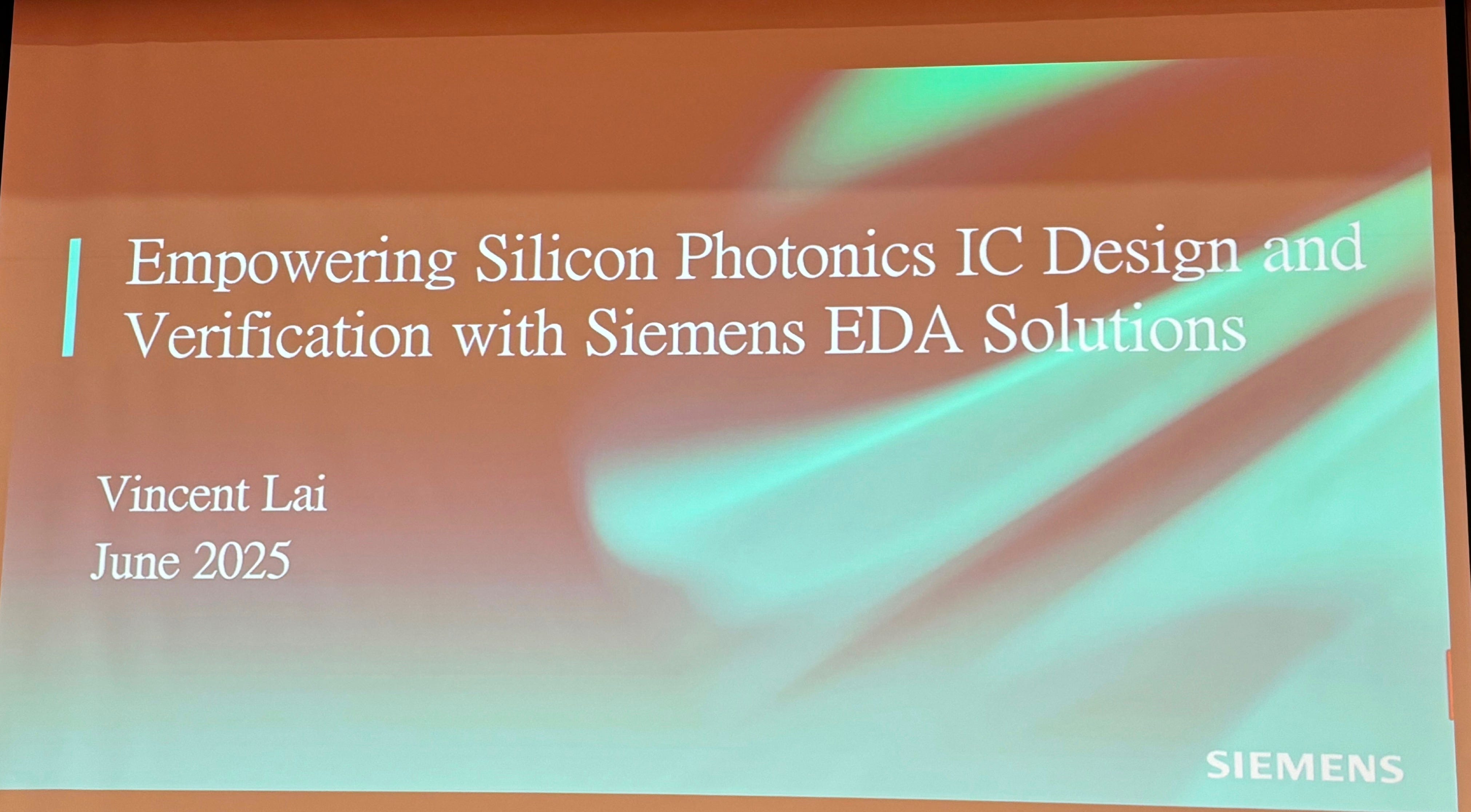
Empowering Silicon Photonics IC Design and Verification with Siemens EDA Solutions
Vincent Lai, Applications Engineer Consultant – Siemens EDA
A deep dive into electro-photonic co-design workflows, IBIS-AMI and SPICE integration, and the critical role of mixed-signal modeling in SiPh circuits.
Challenges in Silicon Photonics Testing and Packaging
Chris Yu, Senior Product Marketing Manager – Suruga Seiki Co., Ltd.
Precision fiber array alignment and mechanical integration solutions for next-gen optical modules in CPO/OIO applications.
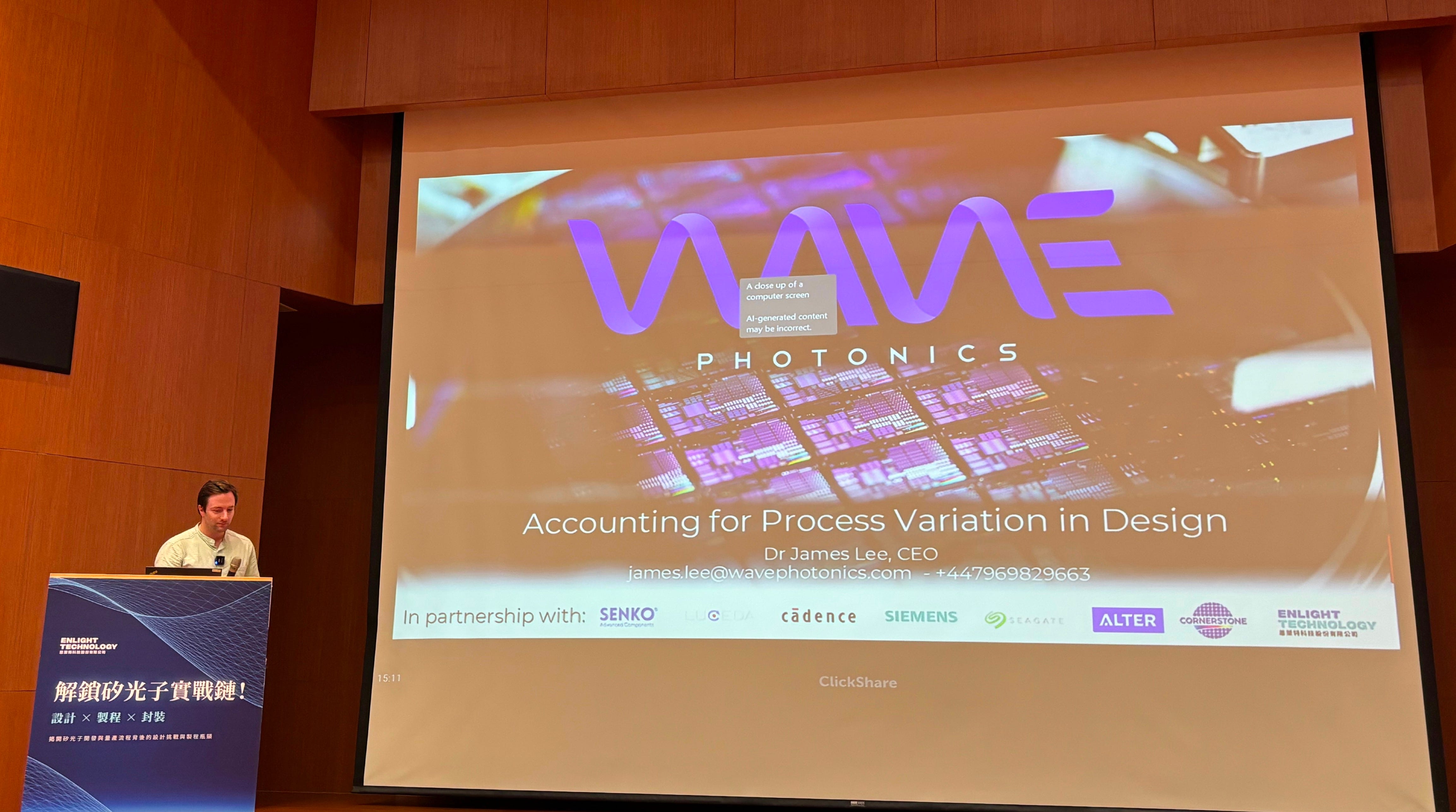
Accounting for Process Variation in Design
James Lee, CEO & Co-founder – Wave Photonics
Cross-platform design strategies for mitigating process variability, with examples from high-speed PIC modules and global research collaborations.
At this seminar, Dr. Sheng-Yu Chen provided an in-depth analysis of the latest developments in the silicon photonics domain, with a particular focus on real-world applications from leading industry players such as TSMC, Intel, and NVIDIA.
TSMC’s COUPE Platform: Innovative Photonic Integration
TSMC’s COUPE (Compact Universal Photonic Engine) platform showcases the company’s cutting-edge approach to silicon photonic integration. By incorporating meta-lens arrays, backside metal reflectors, and anti-reflective coatings, the platform significantly improves the efficiency of grating couplers (GCs). This integration enables coupling losses as low as 0.3 dB, greatly enhancing fiber-to-chip optical interface performance and enabling more efficient optical links within advanced packages.


Intel EMIB: Heterogeneous Integration with Silicon Photonics
Intel’s EMIB (Embedded Multi-die Interconnect Bridge) technology demonstrates strong potential for next-generation photonic-electronic integration. Supporting 2.5D heterogeneous integration, EMIB allows co-packaging of optical I/O chiplets with electronic dies. This architectural synergy is pivotal for the commercialization of Co-Packaged Optics (CPO) modules, particularly in AI workloads and high-performance computing environments.


NVIDIA: Strategic Fiber Choices and Micro-Lens Coupling
In its CPO architecture, NVIDIA opts for Single Mode Fiber (SMF) over Polarization Maintaining Fiber (PMF) to reduce power consumption and simplify module complexity. Additionally, NVIDIA employs micro-lens technology to enhance spatial coupling efficiency, enabling smaller form factors and better overall system performance — a critical enabler for scalable, high-density optical systems.

Advancements in PIC Fabrication and Device Performance
On the process front, Dr. Chen highlighted the use of 193 nm immersion deep ultraviolet (DUV) lithography, which supports fabrication of high-density waveguides and intricate microstructures essential for scaling photonic bandwidth and integration density.
He also emphasized the importance of Ge-based photodetector (Ge PD) development. Key electrical performance parameters — such as dark current, signal-to-noise ratio (SNR), PN junction resistance, and Ids — have a direct impact on the reliability and signal integrity of high-speed photonic receivers, especially at 448 Gbps and beyond. These factors define the success of photonic links in ultra-high-speed systems.
The Critical Role of Silicon Photonics Testing
While silicon photonics design remains the core focus of this seminar, Dr. Chen underscored that testing is equally critical. For ultra-high-speed applications — such as 448 Gbps SerDes — the demands placed on test infrastructure are substantial.


Companies like ficonTEC are addressing this challenge with the development of innovative wafer-level double-sided electro-optical test systems, which allow high-throughput testing of photonic ICs directly at the wafer stage. This capability is vital for improving production yield, reducing cost, and accelerating time-to-market for silicon photonics-enabled systems.
Silicon photonics is rapidly evolving from lab-scale research to commercial-scale deployment, spanning the full spectrum from design and fabrication to packaging and testing. The examples presented from TSMC, Intel, and NVIDIA illustrate the growing role of silicon photonics in enabling AI computing and high-speed data transmissioninfrastructures.
However, realizing the full potential of this technology requires overcoming substantial challenges in design robustness and test infrastructure — challenges that demand collaborative innovation across the entire supply chain.
Next Frontier: Testing Silicon Photonics at Scale
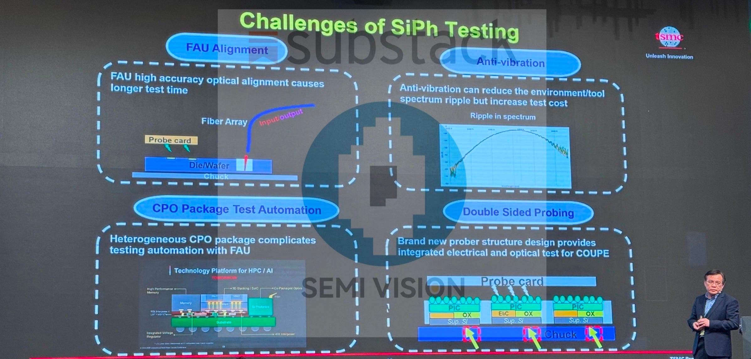
As silicon photonics (SiPh) enters the high-frequency era — driven by 448G SerDes and 800G/1.6T optical modules — testing has emerged as one of the most critical bottlenecks in the path to high-volume manufacturing (HVM). The challenge lies in simultaneously validating both optical and electrical parameters with precision, throughput, and reliability.
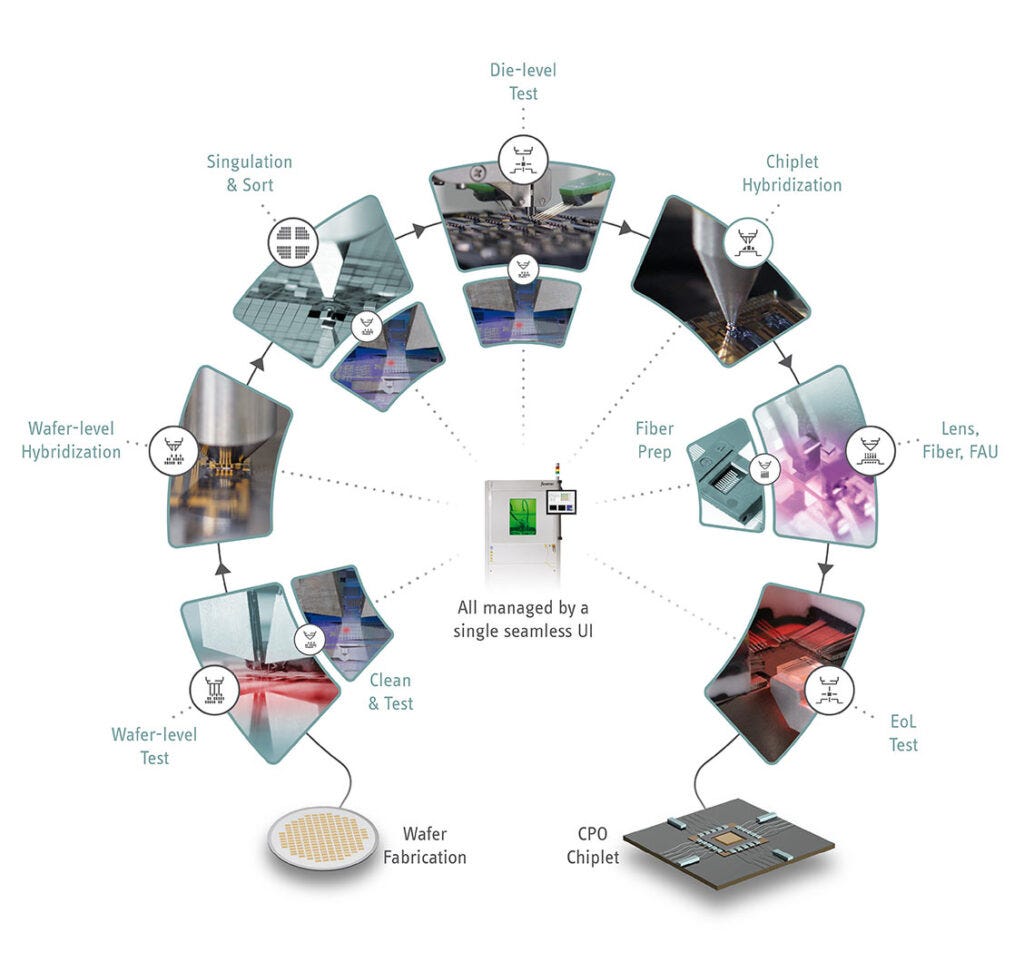
Ficontec’s Breakthrough in Double-Sided Testing
Ficontec has introduced a groundbreaking double-sided electro-optical wafer tester, which enables concurrent testing of Photonic Integrated Circuits (PICs) and Electronic Integrated Circuits (EICs). This advancement represents a pivotal step toward a true one-stop test solution for SiPh-based optical engines, seamlessly integrating into the backend of the packaging process.

The platform has been named a finalist for the 2025 Laser World of Photonics Innovation Awards, and notably, it is the first commercial solution capable of testing TSMC’s COUPE (Compact Universal Photonic Engine) wafers.
Key Product Highlights: 300mm Double-Sided Wafer Test System
World’s First of Its Kind: A 300mm dual-side electro-optical tester purpose-built for AI-driven SiPh applications, fully compatible with existing ATE (Automated Test Equipment) infrastructure.
High-Throughput Capability: Designed to meet the demands of next-gen optical interconnects — such as CPO — this solution supports wafer-level testing of SiPh PICs at production scale.
Double-Sided Design:
Top Side: Executes DC and high-speed electrical probing.
Bottom Side: Employs six-axis active alignment for precision optical probing.
Automation & Accuracy:
Automated wafer handling
Patented vacuum thermal chuck
In-situ fiber array alignment
End-face inspection and probe calibration
Full-chip PIC mapping for optimal test coverage

Strategic Alliance with Teradyne
Seamless ATE Integration: The system is designed for plug-and-play compatibility with standard semiconductor ATE workflows, easing deployment for leading foundries adopting CPO test flows.
Joint Development: Teradyne and ficonTEC have announced a co-developed high-capacity double-sided wafer probe solution, engineered specifically for the demands of CPO manufacturing.
Global Deployment and Roadmap
Installed Base: ficonTEC has over 1,400 systems deployed worldwide, supporting high-density interconnect testing, including 400G, 800G, and 1.6T CPO formats.
Regional Expansion: ficonTEC is strengthening its support networks across Taiwan, Korea, Israel, and the U.S., targeting regions central to the AI compute ecosystem.
Future Development:
Single-sided wafer test systems
Die-level and module-level production testing tools
Hybridized workflows for mixed photonic-electronic integration
Global Silicon Photonics Test Ecosystem: Key Players
The current global supply chain of SiPh test solutions includes:
Teradyne
Advantest
FormFactor
ficonTEC
Suruga Seiki (Taiwan)
In Taiwan, a new wave of domestic suppliers is emerging — focusing on automated alignment systems, high-frequency probing, fiber array integration, and CPO-specific test platforms. These developments are expected to foster complementary ecosystems with international players.
Looking Ahead: Laser World of Photonics 2025
The upcoming Laser World of Photonics exhibition in Germany (June 2025) will serve as a critical vantage point for observing the evolution of SiPh test and packaging infrastructure. The event will showcase:
Automated SiPh probing platforms
Optical alignment modules
3D AOI (Automated Optical Inspection)
High-speed test instrumentation
SemiVision will provide focused updates and analysis on key players and technologies unveiled at the show.
For Paid Members, SemiVision will discuss topics on
Overcoming Electronic Interconnect Bottlenecks
TSMC and Avicena Collaboration
Huawei’s Ascend 910C in all optics architecture
Industry Shift Toward Co-Packaged Optics (CPO)
The Necessity of Photonic Design Automation (PDA)
Ecosystem Collaboration: Building the Foundation for Scalable Photonics
From Concept to Mass Production: Photonics as the AI Enabler
Silicon Photonics and Waveguide Design: Corner Rounding and Coupling Efficiency Enhancement
Optical Interconnect Technologies for Data Centers: Comparing LPO and CP
China’s Optical Module Industry: A Global Powerhouse
AI Compute Showdown: Huawei CloudMatrix 384 vs. NVIDIA GB200 NVL72
Design and Simulation: Co-Design of EIC and PIC
Design Tools and Ecosystem: PIC Studio and Simulation Platforms
Extending EDA from IC to PIC: Siemens’ Approach to Photonic Design Automation
Core Differences Between EIC and PIC Design
Siemens’ Key Functionalities for PIC Design
Equation-Based DRC: A Novel Approach to Photonic Rule Checking
Toward Scalable PIC-EIC Co-Design
Wave Photonics: Advancing Process-Aware Design for Photonic Integrated Circuits
Process Variation and the Need for Robust PIC Design
Reducing Sensitivity to Process Variation through Co-Optimization
Strategic Implications in Wave Photonic


