From Custom SRAM to Optical SerDes: How Marvell Builds the Data Highways for AI Chips
Original Articles By SemiVision Research (Marvell , TSMC , AWS ,Microsoft ,Nvidia, Broadcom)
Marvell Leads AI Chip Infrastructure Innovation: A Full-Stack Transformation from Custom XPU to Optical Interconnects
With the explosive growth of generative AI, large language models (LLMs), and bandwidth-intensive inference workloads, global data centers are undergoing a profound transformation driven by fundamental technology shifts. From processor architecture and memory access to interconnect interfaces and advanced packaging, the boundaries of traditional chip design are being redefined. In this context, Marvell positions itself at the core of this revolution with a “full-stack custom platform” approach, integrating design IP, advanced process nodes, packaging, and high-speed interconnects (SerDes / Optical I/O), becoming a powerful enabler of next-generation AI infrastructure.
Surge in AI Infrastructure Capital Expenditure
According to market data cited by Marvell, capital expenditures from the top four U.S. cloud service providers—Amazon, Microsoft, Google, and Meta—for AI infrastructure have been growing at a 46% compound annual growth rate since 2023, projected to reach $327 billion by 2025. This investment wave signifies a clear shift from general-purpose CPU-centric compute toward accelerated architectures centered on GPUs, TPUs, and XPUs—now becoming the new standard in modern data centers.
At the same time, emerging players such as OpenAI and xAI (model-first), Tesla and Apple (application-first), and Sovereign AI pioneers like Humain and Stargate are rapidly developing custom ASICs and memory systems, contributing to a diversified, decentralized, and co-optimized AI infrastructure ecosystem.
Breaking the GPU Monopoly with Custom XPU Architectures
Amid rising chip design and supply chain costs—especially as NVIDIA GPUs remain expensive and scarce—many cloud providers are moving toward in-house ASIC designs to improve performance-per-watt and manage total cost of ownership (TCO). Marvell’s “XPU + XPU Attach” architecture defines two major custom chip domains:
Custom XPU: Tailored compute cores for AI inference, signal processing, or general-purpose compute tasks.
Custom XPU Attach: Supporting components including SerDes, D2D, scale-up fabric, memory pooling controllers, security, and management engines.
This architecture allows Marvell to provide complete core-to-interconnect solutions, offering flexible, customer-specific chip designs. To date, Marvell has deployed 12 sockets (3 XPUs and 9 Attach chips) among the top four cloud providers and 6 additional sockets among emerging hyperscalers, totaling 18 AI acceleration chips in production—evidence of its platform strategy’s broad industry validation.
Full-Stack Technical Superiority: From Silicon to System
Marvell’s strongest competitive edge lies in its ability to integrate from silicon to system across five core pillars:
System Architecture: Assists customers in defining data flow and parallel compute models for optimized SoC architectures.
Design IP: Offers high-performance SerDes, SRAM, memory controllers, and interconnect IPs.
Silicon Services: Supports cutting-edge process nodes (e.g., 2nm, 14Å, 16Å) with advanced logic design capabilities.
Advanced Packaging: Integrates fan-out, 2.5D, CoWoS, and CPO to increase system density and efficiency.
Manufacturing Logistics: Bridges wafer-level manufacturing and system-level SMT assembly for streamlined supply chains.
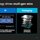
At OFC 2025, Marvell unveiled the world’s first 448G electrical-optical SerDes, supporting next-gen optical interconnect architectures such as CPO, LPO, and OIO. This technology underpins scalable, low-latency, and energy-efficient AI system architectures across rack-to-rack and pod-to-pod deployments.
SRAM and HBM Advancements Paving the Way for Heterogeneous Integration
Memory architecture remains a critical bottleneck for AI chips. In advanced logic nodes, SRAM’s area and power usage become increasingly significant. Marvell addresses this with custom SRAM designs that deliver:
50% smaller area for the same bandwidth
66% lower standby power
17x bandwidth density at the same area
These features are highly suitable for L2/L3 caches, neural caches, and inference weight buffers, and are already integrated into leading AI accelerator designs.
In parallel, Marvell is developing custom HBM systems tightly coupled with its CPO-based photonic packaging platforms. This approach forms a high-performance memory foundation optimized for heterogeneous integration, NoC (Network-on-Chip), and scale-up fabric, enabling low-latency, high-throughput, and scalable compute infrastructure for data centers.
Toward Platform-Centric Chip Design
Marvell’s 2025 technology roadmap outlines three critical vectors for the evolution of accelerated computing:
The shift from single GPU dominance to customizable XPU system architectures
The transition from electrical SerDes to integrated optical interconnects
The move from standard SRAM to custom memory and high-density packaging integration
These trends reflect a fundamental transformation—from point optimization to full-stack system-level design. Only with vertically integrated capabilities in process technology, IP, packaging, and interconnects can future AI infrastructure meet the scale, efficiency, and flexibility required in the Angstrom era.
For Marvell, chips are not just functional units—they are the architectural foundation of tomorrow’s data centers.
For Paid Members, SemiVision will discuss topics on
From Vision to Reality: Marvell’s Transformation Through Cloud-Optimized Silicon
Marvell 2025: Leading the New Era of AI Infrastructure with Full-Stack Technology and Custom Silicon Strategy
Strategic Moves by the Traditional Hyperscalers
The Rise of Emerging Hyperscalers
XPU and Attach Strategy: Marvell’s Dual-Axis Expansion
Decoding the Full Picture Through Sockets: How Marvell Defines Its Influence in the AI Chip Era
Technology Leadership: Comprehensive Deployment Across SerDes, Die-to-Die, and Co-Packaged Optics
Marvell’s Full-Service Offering for AI Chips and Solutions
Why Marvell Wins
Process: From Nanometers to the Ångström Era
IP: World’s First 448G Electrical and Optical SerDes
Packaging: Entering the Battlefield of Advanced Integration
Driving Cross-Generational Success Through Technology
Custom SRAM and HBM: The Architecture Advantage
Custom Memory Strategy as a Core Growth Engine
Marvell’s Business Model and Strategic Shift in Design
Forward-Looking Roadmap: From 3nm to 2nm and the Ångström Era
XPU Attach: The Critical Sibling to XPU in the Modular AI Era
SerDes, Die-to-Die, and Co-Packaged Optics Technologies
Evolution of the Silicon Photonics Platform and Innovations in Advanced Packaging (2.5D, 3.5D, 4.5D)
Impact of Custom SRAM and HBM Architectures on AI Platforms
Facing the Slowdown of Moore’s Law: Marvell’s Platform Strategy for Advanced Process and IP Readiness


