

TSMC’s SoW and the AI Thermal War: Can NVIDIA Keep Up?
Original Article by SemiVision Research (IEEE ECTC , TSMC , Nvidia , Cerebras, Tesla Dojo , Henkel , FiconTEC , Foxconn , Celestial AI , Light matter , Ayar Lab , Ranovus )


Previously, we covered the key concepts of SoW-X (System-on-Wafer eXtreme) as revealed during the TSMC Technology Symposium. Here, we continue by exploring the technical details published by TSMC at the 2025 IEEE ECTC (Electronic Components and Technology Conference).

TSMC’s Thermal Innovations, Photonic Integration, and the Road to SoW
Thermal issues remain one of the most critical challenges for high-performance chips. Excessive heat not only compromises system performance but also threatens the long-term reliability of materials. Recognizing this, TSMC dedicated significant discussion in a recent technical paper to the thermal architecture of its System on Wafer (SoW)platform. As we’ve discussed previously, with the ever-increasing power density of AI chips, TSMC has introduced new thermal interface materials (TIM), lid structures, and novel cooling solutions, which we will cover in more detail in future SemiVision reports.


Meanwhile, TSMC’s ambitions extend far beyond thermal management. We are seeing clear signals of their strategic direction in optical interconnects for AI platforms.


At ISES 2025, TSMC’s VP , Dr. Chiu-Shan Yu , for More-than-Moore technologies presented a deep dive into the TSMC Photonic Platform, explaining how it fits into the broader heterogeneous integration roadmap. The talk covered multiple key aspects of photonic integrated circuit (PIC) manufacturing, reinforcing TSMC’s commitment to silicon photonics as a foundational technology for AI and HPC.


In parallel, TSMC also hosted a dedicated session on PIC and EIC testing technologies, where they highlighted the increasing complexity and importance of testing for optical engines. With NVIDIA now actively developing a standard framework for testing PICs, EICs, and optical engines, we’ve also observed the introduction of double-sided wafer testing—a significant shift in production methodology. SemiVision will soon publish an in-depth analysis on this topic.

During Computex 2025, TSMC and NVIDIA jointly shared their views on the future of silicon photonics for networking, with a keynote delivered by TSMC VP KH Shu. Notably, at IEEE ECTC 2025, Shu’s team published a paper detailing the outstanding performance of TSMC’s Photonic COUPE platform. More importantly, the paper elaborated extensively on PIC reliability analysis, indicating that TSMC is shaping the standards for silicon photonic integration—and cementing its leadership position.

Furthermore, a separate TSMC paper—authored by their advanced pathfinding division—outlined a platform vision that NVIDIA has long sought: a scalable photonic platform where the optical engine is directly integrated into the interposer. This concept is an extension of COUPE and includes robust test strategies. A key takeaway from the paper is TSMC’s focus on how to achieve high-efficiency coupling using FAU (Fiber Array Unit) structures.

To revisit NVIDIA’s 2025 ECTC paper, it’s clear that they are leveraging TSMC’s full suite of advanced packaging and photonics technologies for their optical interconnect solutions. The collaborative puzzle between TSMC and NVIDIA on silicon photonics is quickly coming together.

Ultimately, the convergence point will be where optical engines are co-integrated with TSMC’s SoW (System on Wafer) platform. As a result, TSMC is now extending its iOIS (Integrated Optical Interconnect System) platform architecture into the SoW ecosystem—a strategic evolution with profound implications for the next generation of wafer-scale AI computing.
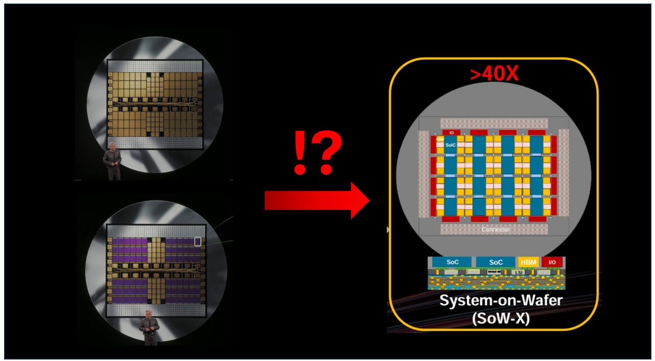
In this paper, TSMC elaborates on its next-generation wafer-level 3DIC architecture, including how SoW-X enables the integration of up to 16 full-reticle ASICs, 80 HBM4 modules, and 2,800 high-speed SerDes channels (each at 224 Gb/s), achieving a total inter-die bandwidth of 260 TB/s and external bandwidth of 80 TB/s. The design showcases a 1.76× improvement in power efficiency, a 46% boost in compute performance, and a 17% reduction in power consumption compared to equivalent networked chiplet systems.


The paper further emphasizes innovations in wafer-level redistribution layers (RDLs), local silicon interconnects (LSI), and multi-die co-packaging, all made possible through system technology co-optimization (STCO). It also highlights advanced thermal modeling and liquid cooling strategies, supporting reliable operation under extreme AI/HPC workloads.
This engineering breakthrough reaffirms TSMC’s leadership in system-level integration and sets a new benchmark for advanced packaging in the AI era.
Deconstructing TSMC SoW-X: The Ultimate Packaging Platform for the AI/HPC Era
As demand surges for Artificial Intelligence (AI) and High-Performance Computing (HPC), the need for ultra-high integration density and massive data throughput has pushed conventional packaging architectures to their limits. To overcome three critical bottlenecks—reticle size, I/O bandwidth, and thermal management—TSMC unveiled a groundbreaking packaging innovation at the 2025 IEEE ECTC: SoW-X (System-on-Wafer, eXtreme).
This architecture marks not just a leap in packaging capabilities, but a tangible realization of wafer-level system integration. SoW-X redefines how logic and memory interact at scale, opening a new chapter in system co-design and packaging for the next generation of AI and HPC systems.
For Paid Members , SemiVision will discuss topics on
Hyperscale System Integration: The Packaging Breakthrough of SoW-X
Redefining the Wafer: Multi-Layer RDL + LSI Architecture for Full-Wafer High-Speed Interconnect
Key to SoW-X High-Speed Channel Design: SerDes, Eye Diagrams, and Signal Integrity Optimization
Tackling Thermal Challenges with Zone-Based Liquid Cooling Architecture
From Packaging Materials to System Co-Optimization: The Foundational Pillars of SoW-X
TSMC * Nvidia : Entering the New Era of System-Level Packaging
Summary : TSMC’s SoW-X: A Breakthrough in Wafer-Level System Integration for the AI/HPC Era