From Thermal Budget to Competitive Edge: How TSMC Builds a Cooling Moat for AI Chips to Strengthen NVIDIA’s Market Leadership
Original Articles by SemiVision Research (IEEE ECTC , TSMC , Nvidia)
Under the wave of generative AI, AI chips are rapidly evolving toward “ultra-large die area, high bandwidth, and high power consumption” designs. This shift brings with it an increasingly critical challenge: the thermal budget bottleneck. As transistor density approaches its physical limits, internal heat flux becomes harder to dissipate efficiently. At that point, thermal management is no longer just a design consideration—it becomes a fundamental challenge of manufacturing and packaging.
In this race, TSMC, the world’s leading semiconductor foundry, is redefining what advanced packaging and thermal solutions can offer. Through technologies such as CoWoS-R, SoIC, IMC-Si, and BSPDN (Backside Power Delivery Network), TSMC is building a thermal management moat for the next generation of AI chips.
More importantly, these innovations are not just technical milestones—they are strategic enablers for leading AI chipmakers like NVIDIA to reinforce their dominance. This article offers an in-depth look at TSMC’s systemic approach to thermal packaging—from materials R&D and thermal simulation to direct liquid cooling implementation—revealing how future chips will strike a stable and reliable thermal balance amid rising performance and power demands.
The thermal budget has become one of the most formidable physical challenges in today’s AI chip design. With the rapid evolution of generative AI, large language models, and high-performance inference engines, AI chips are trending toward larger die sizes, higher bandwidth, greater compute density, and inevitably, higher power consumption. However, all of this hinges on the capabilities of wafer fabrication and advanced packaging—and the vast majority of ASIC designs for AI acceleration are built upon TSMC’s leading-edge logic processes and packaging platforms.
Currently, CoWoS (Chip-on-Wafer-on-Substrate) has become the dominant packaging architecture for AI, supporting the integration of multiple dies and high-bandwidth memory (HBM). Looking ahead to even more advanced AI chip designs—such as ultra-large SoCs, multi-reticle stitching, and chiplet-based systems—TSMC is advancing 3D packaging technologies like SoIC (System on Integrated Chips), enabling shorter interconnects, lower latency, and improved electrical and thermal performance.
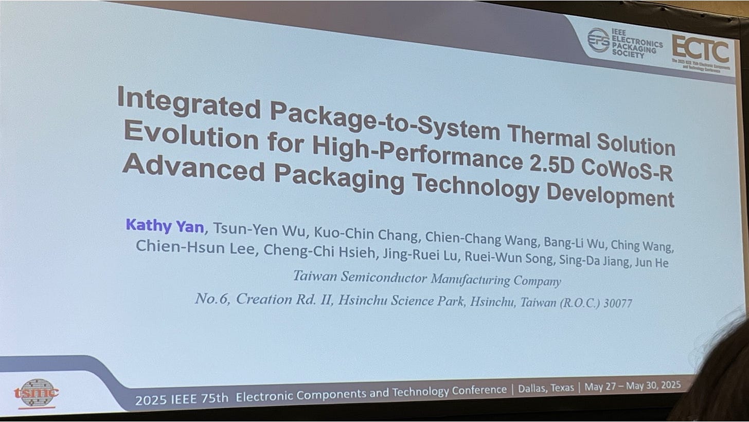
In this analysis, we focus on a pivotal technical paper presented by TSMC at the 2025 IEEE ECTC, which systematically outlines a comprehensive thermal solution spanning the chip level, package level, and system level. The study centers around how the CoWoS-R–based 2.5D packaging architecture effectively addresses thermal conduction and reliability challenges under high power density conditions.
Traditional cooling approaches—such as the TIM1 + Lid + TIM2 stack—are increasingly inadequate for AI chips with thermal design power (TDP) reaching into the kilowatt range. Through both simulations and empirical data, TSMC demonstrates that integrating a Si-integrated Micro Cooler (IMC-Si) with direct liquid cooling into next-generation chip packaging significantly reduces thermal resistance. This innovation enables stable operation beyond 2 kW, delivering higher thermal efficiency and improved packaging reliability.
This transformation represents more than just a technical upgrade—it signifies a restructuring of the entire semiconductor supply chain. From material selection and process integration to packaging architecture and system-level thermal co-design, achieving these advancements requires deeper collaboration and interdisciplinary innovation.
TSMC also underscores its strong commitment to materials science. It has conducted microscopic studies on the behavior of thermal interface materials (TIMs), tackled edge-effect-induced thermal resistance variations, and published multiple studies addressing the thermal challenges of its System-on-Wafer (SoW) platforms. These efforts collectively highlight the company’s broad and deep investment in advancing thermal management technologies.
In this article, we take a deep dive into TSMC’s engineering perspective on Thermal Interface Materials (TIMs), exploring how future AI chips, faced with escalating power demands, must return to the fundamentals of thermal physics—specifically, Fourier’s Law of Heat Conduction—to redefine the overall approach to thermal interfaces and packaging design. This is not only crucial for ensuring chip-level stability but also has profound implications for system architecture and the energy efficiency of data centers at large.
Within the realm of high-performance packaging and AI chip thermal management, TIMs serve as one of the most critical junctions between the silicon die and the external cooling solution. The effectiveness of this interface directly impacts package-level thermal resistance, system reliability, and overall yield.
Recognizing this, materials suppliers such as Henkel have aggressively expanded into advanced semiconductor markets. By developing a comprehensive portfolio tailored to various packaging architectures and power profiles, they aim to address the increasingly severe thermal budget constraints. These innovations in TIMs—ranging from high-conductivity pastes to ultra-thin films optimized for high-power density applications—play a pivotal role in enabling next-generation AI systems to scale reliably under extreme thermal loads.
For paid members, SemiVision will provide an in-depth discussion on TSMC’s thermal solutions for next-generation AI chips, along with the latest innovations in advanced thermal interface materials.
Thermal issues can significantly impact AI chip performance due to the thermal sensitivity of CMOS devices
Thermal issues can significantly impact AI chip performance due to the thermal sensitivity of CMOS devices
Advanced packaging is no longer just about packaging—it now involves the integration of materials and system-level considerations
Holistic Approach: Package + System Co-Design
TIM Material Innovations Across Four Key Packaging Architectures for High-Power Dissipation: From Fundamental to Advanced Designs
Thermal Interface Material (TIM1) Configurations for High-Power Packaging: From Conventional to Advanced
Industry Landscape and Technical Progress in Si-Integrated Micro-Cooler (IMC-Si) and Lidless Packaging Technologies
Industry Commentary and Development Outlook
Future Direction: Co-Design Across Packaging, Fluidics, and System Architecture
Thermal Interface Material Comparison
TSMC’s Next-Generation Direct Liquid-Cooling Packaging Solution: Si-Integrated Micro Cooler (IMC-Si) Presented at 2025 IEEE ECTC
Core Concept: Microstructured Silicon Meets Direct Liquid Cooling
Thermal Management Evolution in High-Power Packaging: From Conventional TIMs to IMC-Si
Conclusion from TSMC’s 2025 IEEE ECTC Presentation: A Multilevel Thermal Co-Design Approach for HPC Systems
To gain a better understanding of the thermal budget in AI chips, you are encouraged to consult the relevant articles for comprehensive information


