

Next-Gen AI Cooling: Moving Toward Microchannel-Based Architectures
Original Articles By SemiVision Research (IEEE ECTC , KLA , EVGroup , Meta , TSMC ,HP , Google , ASE , SEMI , Henkel)


At the 2024 IEEE ECTC conference, a highly notable technical paper titled “Moving Towards Microchannel-Based Chip Cooling” was presented. This paper is of exceptional value not only for its technical depth, but also because of the prestigious affiliations of its authors, who come from leading global organizations such as SEMI, KLA, EVG, Meta, TSMC, HP, Google, and ASE.

TSMC
TSMC showcased their “Si‑Integrated Micro‑Cooler” at IEEE ECTC 2024, presenting wafer‑level microchannels etched directly into the backside of active chips using MEMS/DRIE. These channels are integrated with CoWoS packaging and interposers to support heat fluxes up to 2.6 kW while maintaining ΔT ≈ 63 °C . Ongoing work includes trench, pillar, and planar microchannel variants, with pillar-based structures showing the best performance.
EVG (EV Group)
EVG provides the core wafer-bonding technology required for embedding microchannels at wafer scale. Their GEMINI and EVG501 systems support high-force, large-area bonding (up to 350 kN), essential for integrating microchannel wafers between SoC and HBM . Their presence at ECTC 2024 highlights their leadership in wafer-level bonding for heterogeneous integration .

KLA (SPTS Technologies)
Through SPTS, KLA supplies advanced MEMS process tools critical for microchannel fabrication. Their DRIE systems — based on the Bosch process — are regarded as industry leaders for achieving high-aspect-ratio features (like deep trenches and TSVs) . These tools are vital for producing reliable microchannel structures in silicon.

HP
HP’s long-standing expertise in MEMS-based printhead manufacturing (with thousands of microfluidic nozzles per chip) shows deep experience in large-scale backside etching and fluidic control surfaces . Although not actively marketing chip cooling solutions, their MEMS heritage suggests they could adapt their microfluidic technologies for thermal management applications.
Meta, Google, ASE
While specific microchannel initiatives by Meta or Google are not public, both companies are active collaborators in ECTC and advanced packaging R&D. ASE (Amkor/ASE Group) — a major OSAT player — is positioned for system-level integration, including wafer-to-wafer bonding, interposer assembly, and final packaging necessary to implement microchannel systems .
Purpose and Industry Significance
The core objective of this study is to address the thermal bottlenecks facing next-generation AI chips and to propose feasible, scalable solutions for the future. As AI models expand into the trillion-parameter era, the power density of a single SoC has exceeded the capabilities of traditional thermal modules. Air cooling and single-point liquid cooling are no longer sufficient, especially in the context of 3D-stacked advanced packaging. To tackle this challenge, the team proposes a novel architecture centered around wafer-level microchannel cooling.
Key Technologies and Ecosystem Participation
The paper outlines several key technological innovations and highlights the involvement of an extensive supply chain to support manufacturable solutions, including:
Wafer-on-Wafer (WoW) Bonding: SoC and HBM wafers are bonded at the wafer level, with a MEMS-based microchannel wafer inserted in between. This bonding is supported by EVG (EV Group), a leading provider of wafer bonding solutions.
MEMS-Based Microchannel Fabrication: To create fluidic channels within silicon wafers, deep reactive ion etching (DRIE) processes are applied. Key equipment and metrology providers include SPTS Technologies (now part of KLA) and KLA itself.
System-Level Package Integration: The architecture integrates SoC, HBM, and a microchannel wafer into a single stack, mounted on an interposer to form a full system-in-package. Foundries and OSATs such as TSMCand ASE play critical roles in backend processing and advanced thermal packaging.
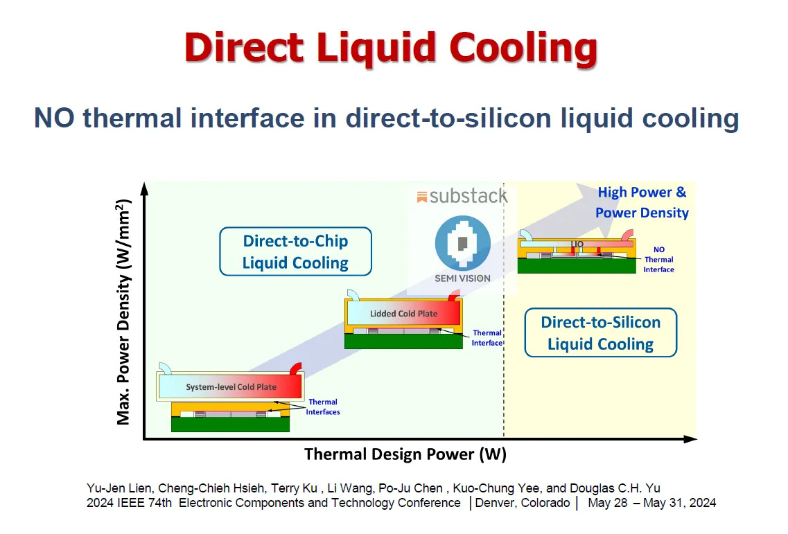
TSMC’s Strategic Participation: From TIM Challenges to No-TIM Innovation
The paper also offers deep insights into a long-standing bottleneck in chip thermal management: the limitations of thermal interface materials (TIMs) in terms of thickness and heat conduction.
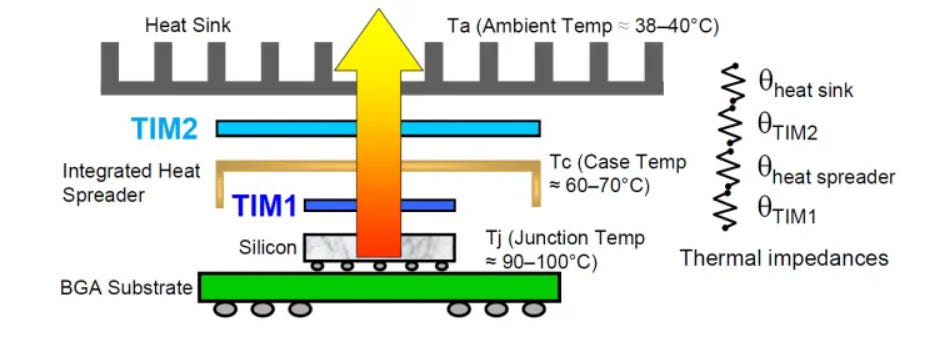
Traditional structure: AI Chip → TIM1 → Lid → TIM2 → Cold Plate
TIM1 (between die and lid) and TIM2 (between lid and cooling module) significantly influence total thermal resistance.
Voids, poor adhesion, and non-uniform contact in TIM layers often degrade thermal performance.
To address this, TSMC’s contribution to the paper includes a forward-looking proposal of a “No-TIM” architecture, which eliminates the TIM layer entirely. Instead, it introduces direct thermal contact between the chip backside and the cooling structure, significantly reducing interface thermal resistance. This concept aligns with other papers TSMC has presented at ECTC, emphasizing its strategic investment in thermal co-design at the package level.


Closing Thoughts and Technical Outlook
This paper is an outstanding example of international, cross-disciplinary collaboration across the semiconductor ecosystem. It illustrates that future semiconductor innovation will not be defined solely by signal integrity or packaging density, but also by thermal architecture and co-design.
In tomorrow’s AI computing era, the question is no longer just “how many chips can you stack?”, but rather, “how well can you dissipate the heat from those high-performance chips?” This is where SoW architectures, microchannel integration, No-TIM strategies, and embedded liquid cooling will define the next competitive frontier.


The core challenge in AI chip thermal management today lies squarely within the chip itself. Therefore, it is crucial for foundries to propose systematic solutions from their end of the value chain. The following details further elaborate on this point, with a focus on TSMC’s efforts under silicon-based architectures—specifically in the exploration of microchannel cooling, DRIE/MEMS applications, copper pillar array design, TIM material challenges, and No-TIM architectures. These thermal solutions are applicable not only to SoW and CoWoS but also to silicon photonics-integrated advanced packaging.


As artificial intelligence computing enters the era of trillion-parameter models—with training power consumption reaching hundreds of kilowatts—the design bottleneck for AI chips is shifting from compute capacity and memory walls to another invisible barrier: the thermal wall. Today’s mainstream cooling technologies, including air and traditional liquid cooling, are increasingly inadequate in handling heat flux densities exceeding 300 W/cm². Moreover, the uneven thermal distribution across AI chips introduces additional complexity to thermal management. Conventional heat dissipation structures, such as “AI Chip → TIM1 → Lid → TIM2 → Cold Plate,” introduce multiple thermal interfaces that significantly increase thermal resistance, limiting both heat transfer efficiency and overall system performance.
In response to this thermal crisis, the industry is now shifting its focus upstream: thermal path design should be initiated at the advanced packaging and wafer manufacturing stages, rather than being treated as a passive challenge at the backend. This article stands at that inflection point—examining innovations in wafer-level integration, MEMS fabrication, and microchannel-based liquid cooling systems, with a particular focus on how TSMC and other leading foundries are spearheading system-level thermal breakthroughs.
The article opens by highlighting the promise of wafer-level microchannel structures—such as those fabricated using DRIE (Deep Reactive Ion Etching) techniques to create silicon through-holes or channel features. These channels enable liquid coolant to be introduced directly adjacent to heat sources, dramatically shortening the heat transfer path. Such a design not only supports advanced packaging techniques like CoWoS and 3DIC, but also allows for localized cooling at hotspots, reduces overall thermal resistance, and mitigates thermal fluctuations, enabling high-efficiency on-chip convective cooling. TSMC’s pillar-based microchannel design, for instance, demonstrates the ability to handle thermal loads of up to 2.6 kW, while keeping temperature differentials within 63 °C.
Additionally, the article explores a transformative shift in wafer-level thermal design: the No-TIM architecture. Unlike traditional TIM materials, which are prone to void formation, adhesion issues, and thermal aging, the No-TIM approach integrates cooling channels directly into the backside of the silicon chip. This allows coolant to directly interface with the heat-generating regions, eliminating intermediate materials and their associated thermal resistance and reliability risks—thereby opening a new thermal pathway for future high-power AI chips.
The article also addresses the mechanical reliability concerns arising from high heat flux and materials mismatch. It explores strategies such as structural optimization (e.g., Cu pillar arrays, low-pressure-loss channel designs) and system-level thermal simulation, aimed at ensuring long-term stability under extreme operating conditions.
Ultimately, this article is not just about technological advancement—it reflects a fundamental shift in design philosophy: foundries are no longer just manufacturers, but integral architects of thermal management for AI chips. As we enter the era of 3D ICs, Chiplets, and System-on-Wafer architectures, only by embedding thermal optimization at the silicon level can we truly overcome the limits of heat.
This is a revolution at the intersection of packaging, silicon process engineering, and liquid cooling innovation. It is a philosophical evolution from “cooling” to “thermal co-design”—and it marks a critical leap forward in enabling the future of AI.


While wafer-level liquid cooling and No-TIM architectures are gaining traction as revolutionary solutions, Thermal Interface Materials (TIMs) remain an indispensable part of today’s thermal management strategies—especially given the realities of chip packaging, manufacturability, and system integration. Among TIM providers, Henkel has emerged as a key player, advancing both material performance and process integration for high-power AI chip packaging.
As AI chips evolve toward high-density, high-power, and multi-die stacking configurations—such as Chiplet + HBM + 3D integration—thermal management has become a central concern in packaging design. Within this architecture, TIMs serve a critical function: transferring heat from chips or stacked modules to heat sinks, cold plates, or liquid cooling systems with minimal thermal resistance.
Henkel, a global leader in adhesives and materials solutions, has developed a comprehensive and modular ecosystemfor TIMs under its well-known brands such as Bergquist and Loctite. Henkel’s TIM portfolio spans six major categories: gap fillers, gap pads, SIL pads, thermal adhesives, phase change materials (PCM), and thermal greases. These materials are widely deployed across high-end processors, 5G base stations, data centers, automotive electronics, and industrial control systems.
On the technology front, Henkel continuously pushes the performance boundaries of TIMs. A prime example is its next-generation Bergquist Hi Flow THF 5000UT phase change material, which remains solid at room temperature and melts upon heating. This material achieves a very low thermal resistance of 0.04°C·cm²/W and thermal conductivity over 8.5 W/m·K with bondline pressures under 10 psi—making it particularly suitable for fragile, high-performance AI chips where ultra-thin and low-pressure TIM1 layers are critical.
For TIM2 interfaces, which span from chip lid to cold plate, Henkel offers a variety of gap pad solutions designed to accommodate mechanical compliance and absorb thermal stress. The TGP 10000ULM pad, with a thermal conductivity of up to 10 W/m·K, supports high-power modules, especially in data center and automotive environments. The product line includes ultra-soft, UL-certified, and electrically conductive options to address varying thickness and compliance needs.
Beyond raw material performance, Henkel places strong emphasis on process-friendly and automation-compatible designs. The THF series PCMs can be pre-applied to lids or cold plates, avoiding issues like manual grease application, air gaps, and inconsistent contact. Gap fillers can be dispensed, printed, or transfer-applied using dual-component systems to meet the high-precision requirements of advanced packaging facilities.
Henkel’s TIM development aligns with the most critical trends in AI/HPC packaging, including:
High-conductivity phase change materials for ultra-thin TIM1 applications.
Soft and conformal gap pads/fillers for TIM2 heat spreading.
Interface materials compatible with microchannel liquid cooling structures.
Multifunctional TIMs for next-generation architectures such as Co-Packaged Optics (CPO) and System-on-Wafer (SoW).
In summary, Henkel is playing an increasingly strategic role in AI thermal solutions through material innovation, low-pressure bonding design, automation readiness, and high-power system compatibility. As chip power density continues to climb, Henkel’s TIM technologies are poised to remain a foundational element in future AI packaging thermal designs.


For Paid Members , SemiVision will discuss topics on
Foundry Perspective: Why Chip Thermal Architecture Must Be Led by the Foundry Side
MEMS Architecture may be a good choice in liquid cooling system
Microchannel Liquid Cooling Concept drive next ai chip generation
MEMS/DRIE Process and Silicon Stress Management
What is DRIE (Bosch Process)?
Copper Pillar Array for Enhanced Thermal Convection Paths
TIM Material Research vs. No-TIM Architecture Innovation
System-Level Co-Optimization: Foundry-Led Direction for Future Thermal Packaging
AI Era Heat Flux Challenge: Hotspots Entering Overheating Zone
TSMC’s Perspective: Silicon Cooling Die and Chip-Level Thermal Solutions
What Is Thermal Budget?
Why Is Thermal Budget Important?
Understanding Thermal Budget: A Critical Constraint in Chip and System Design
System-Level Power Considerations
Challenges to Thermal Budget and Microchannel Limitations
Recent Breakthroughs: Advanced Solutions to Push the Thermal Budget Further
Advancing Toward Microchannel-Based Chip Cooling: A Thermal Revolution for the AI Era
Microchannel Geometry and Packaging Challenges