

TSMC: Acceleration of Taiwan’s “Local-to-Local” Semiconductor Strategy
Original Articles By SemiVision Research (SEMICON, TSMC, ASE, PTI, Corning, Besi, K&S, ASMPT, Globalfoundries, Onto, DISCO, Henkel, Globalwafers, KINK)

At this year’s SEMICON Taiwan 2025 Technology Forum, AI/HPC was once again reaffirmed as the central driver behind the evolution of semiconductor manufacturing, advanced packaging, and testing technologies. The core discussions focused on CoPoS, 3D hybrid bonding, N2 and GAA processes, paradigm shifts in testing, and CPO.

First, CoPoS (Chip-on-Panel-on-Substrate) remains in the pilot production and validation stage. While TSMC has already confirmed the 310×310 mm panel substrate size, the overall ecosystem is still immature. A realistic timeline for volume production is closer to 2029–2030. At the same time, 3D hybrid bonding is shaping a blueprint for so-called “3.5D packaging.” Both AMD and Broadcom have showcased real-world deployments, and TSMC’s SoIC platform is set to expand further, driven by large customers such as Apple and Meta. However, short-term visibility for equipment orders is lower than expected.
On the logic process and materials innovation side, TSMC confirmed that N2 will enter mass production in 2025, with roadmaps advancing toward A16 with backside power delivery and the A14 node, emphasizing the importance of DTCO/STCO co-design and Ångström-level precision control. In parallel, the testing industry is undergoing a value reassessment: as chip size and complexity continue to grow, “Shifting Left” in testing is becoming the new standard. TSMC and ecosystem partners showcased advanced probing solutions and AI-assisted approaches.
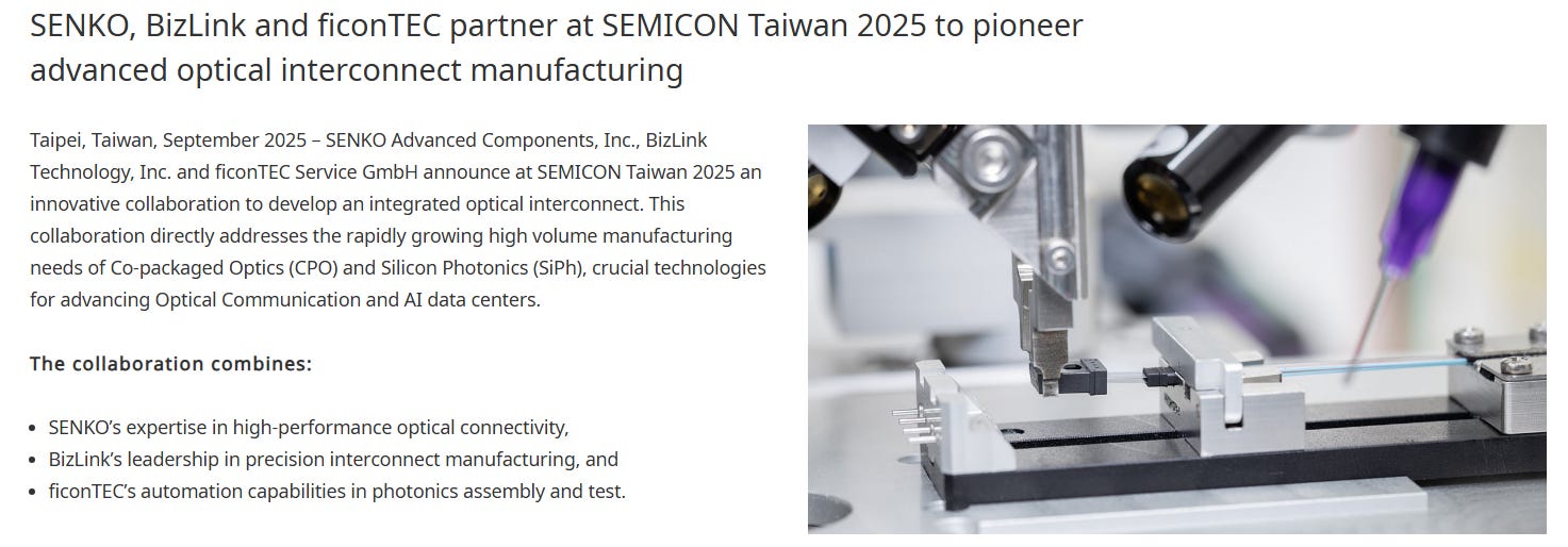
Finally, Bizlink used the exhibition to highlight its entry into new domains such as CPO and semiconductor process equipment (SPE). Partnering with SENKO and ficonTEC, Bizlink is gradually becoming part of TSMC’s CPO supply chain, evolving from cable manufacturing to full-system integration — underscoring its strategic transformation and growth potential.

Overall, SEMICON Taiwan 2025 sent a clear signal: as AI/HPC drives ever-larger die sizes and compute demands, the value of packaging, testing, and optical interconnects will rise sharply, with Taiwan’s supply chain actively investing in new technologies to navigate this structural transformation.
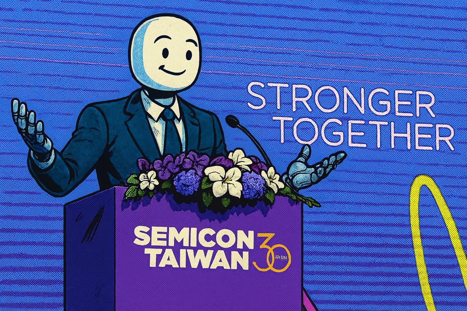
Acceleration of Taiwan’s “Local-to-Local” Semiconductor Strategy:
Materials Self-Sufficiency, Localization of Advanced Packaging, and the Kickoff of CoPoS

In recent years, geopolitical risks in the global semiconductor industry have continued to rise, making supply chain security no longer a back-end consideration but a core element of strategic planning. As a global semiconductor hub, Taiwan made a clear statement at SEMICON Taiwan 2025 through its “Local-to-Local” policy: the future strategy is not only to consolidate its leading position in wafer manufacturing but also to comprehensively expand in three critical areas—materials self-sufficiency, localization of advanced packaging, and acceleration of CPO/CoPoS platforms—in order to build a complete and resilient local ecosystem.
At SEMICON Taiwan 2025, the technical forum once again delivered a clear message: AI and HPC are redefining the core driving forces of the semiconductor industry. As generative AI, inference, and training workloads continue to expand, the scale of model parameters is rapidly leaping from tens of billions to the trillion level. The compute density and power consumption of a single GPU/AI accelerator have already surpassed the kilowatt-class threshold, while memory bandwidth requirements have broken through 10 TB/s. This is forcing a profound restructuring across the entire supply chain—from front-end wafer manufacturing to back-end packaging and testing.
The forum highlighted critical paths that will shape the competitive landscape of the next decade: CoPoS (Chip-on-Panel-on-Substrate), 3D Hybrid Bonding, N2 and GAA nodes, paradigm shifts in testing, and CPO (Co-Packaged Optics) integration.
In advanced process technology, the N2/GAA rivalry between TSMC and Intel is not only about yield and transistor density, but also about whether future system architectures can sustain the massive data throughput required for AI workloads. In packaging, 3D Hybrid Bonding and the expansion of CoWoS/FOPLP have become strategic cornerstones for integrating HBM, SerDes, and GPU/AI ASICs. Meanwhile, panel-level CoPoS packaging represents liberation from reticle limits, enabling ultra-large-area interconnects and cost-efficient, high-volume solutions.
In testing and inspection, traditional electrical testing methods are no longer sufficient to handle the complexities of electro-optical heterogeneous integration, driving adoption of optical metrology, adaptive test platforms, and AI-driven defect analytics as new standards. On the system interconnect front, the rise of CPO and OIO (Optical I/O) directly challenges the physical limits of copper. By co-packaging optical engines with ASICs, they can cut long-distance SerDes losses, deliver ~3.5× energy-efficiency gains, and bring a revolutionary shift to data centers and supercomputing clusters.
Taiwan plays a pivotal role in this structural transformation. Historically, Taiwan’s global semiconductor position was anchored by wafer manufacturing (with TSMC at the core). Today, however, its strategic footprint extends across the entire supply chain. Through a “Local-to-Local” localization strategy, Taiwan is strengthening self-sufficiency in upstream materials such as EUV photoresists, photomasks, chemicals, CMP consumables, and wet process chemicals—reducing reliance on single international suppliers and building diversified supply networks to mitigate geopolitical risks.
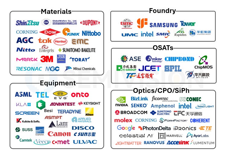
At the same time, advanced packaging capacity is expanding rapidly. Industry leaders such as TSMC, ASE, and Powertech are scaling platforms including CoWoS-S, CoWoS-R, InFO, FOPLP, and SoIC-X, building new facilities in Kaohsiung, Taichung, Hsinchu, and Central Taiwan. These are being integrated with liquid cooling, microfluidic thermal solutions, and 3D integrated testing to form a complete AI/HPC packaging cluster.

In photonics, Taiwan is co-developing CPO and OIO platforms with NVIDIA, Broadcom, Marvell, while also attracting optical connector and FAU players such as Bizlink, FOCI, Teramount, and Senko to set up locally. Combined with academic institutions like ITRI, NCTU, and NCKU, Taiwan is gradually forming a silicon photonics and optoelectronic packaging cluster.

Going further, the Taiwanese supply chain is evolving from pure contract manufacturing to vertical collaboration across design–manufacturing–testing–packaging–materials. Through co-design (DTCO, STCO), EDA platforms, and advanced testing services, Taiwan is constructing a comprehensive strategic fortress spanning materials, equipment, process, packaging, and photonic integration.
This means Taiwan is no longer just the global hub for wafer manufacturing—it is also becoming the core node for next-generation AI infrastructure, optical interconnects, and heterogeneous integration platforms, with an irreplaceable strategic role. In other words, Taiwan will serve as a dual engine for both Moore’s Law extension (advanced nodes) and Beyond-Moore innovation (packaging and photonic integration), ensuring its continued leadership in the global AI/HPC era.
For Paid Members, SemiVision will discuss topics on
Materials Self-Sufficiency: Tackling the Bottlenecks First
Localization of Advanced Packaging: Dual-Track Expansion in Capacity and Equipment
CPO / CoPoS Takeoff: Building the Next-Generation Platform
From Slogan to Execution: Taiwan’s New Semiconductor Strategy
Semicon Taiwan’s Silicon Photonics Forum and the Road Ahead
GlobalFoundries’ Fotonix Platform
New Highlights and Trends Observed at Semicon Taiwan
Future Directions and Key Opportunities
PTI and ASE in FOPLP: Strategies and Key Technologies
PTI’s FOPLP Development Focus
ASE’s Commitment and the VIPack™ Platform
The Relationship Between FOPLP and Optical Engines
AGC: Applications for Glass-core substrate
Senko: Expanded Beam , Detachable connectors for CPO
COMET :3D X-ray solution for 3D Packing
Heterogeneous Integration Tech Forum : Glass Core / Glass Substrate Supply Chain and Technical Perspectives
3D X-Ray Inspection / Comet Yxlon’s CA20 System and Advanced Testing Needs
Why 3D X-Ray Is Critical in FOPLP / Advanced Packaging Environments
Corning’s Strategy in Glass Materials and Applications in Glass Substrate / Glass Core
How Glass Substrate / Glass Core Are Applied (Integration with FOPLP / Advanced Packaging)
Semiconductor Supply Chain Driving Next-Generation Advanced Packaging
Semiconductor Supply Chain Driving Next-Generation Advanced Packaging (KINK &PSI)
Process Equipment: Extending Front-End to Back-End (LAM & TEL & SCREEN )
Bonding and Packaging: The Core Driver of Interconnect (EVG & BESI & ASMPT & HANMI & K&S)
Metrology and Inspection: Guardians of Yield (ONTO & DISCO & Lasertec )
Company Updates / SEMICON Taiwan Highlights (SUSS MicroTec & Advantest & TEL)
Materials / Supply Chain & Overall Exhibition Trends
Local Supply Chains Driving the Infrastructure for Advanced Packaging (G2C+ & KINK )
A New Chapter in Advanced Packaging for the Chiplet Era
EVG and Hybrid Bonding Leadership
Fluxless TCB and D2W Hybrid Bonding Expansion
Market Outlook: Dual-Track Competition
Core Technical Challenges & Future Watch Points
Henkel’s Material Strategy and Advanced Packaging Reliability for AI Chips
Inspection and Testing: The Quality Safeguard of Advanced Packaging
Inspection & Testing Supplier Landscape and Trends
Breakthrough in Silicon Photonics Testing: Double-Sided Testing as a New Benchmark for PIC/EIC Reliability (FiconTEC)
Key Highlights of GlobalWafers’ 12-inch SiC Wafer Technology
The Next Frontier of Chip Technology: Radical Innovation for Unprecedented Performance
Diamond on Chip: A Revolution in Thermal Management
Comparative Analysis of Next-Generation AI Accelerator Specifications
National Strategy and Industry Response
SemiVision believes that the strategic significance of CPO is driving the acceleration of the optical interconnection industry with unprecedented force. In AI/HPC application scenarios, traditional copper interconnects are reaching both physical and energy-efficiency limits: high-speed SerDes, when transmitting across packages or modules, must rely on compensating circuits such as retimers, equalizers, and pre/post-emphasis to maintain signal integrity (SI). However, these solutions come at the cost of high power consumption and latency, making it increasingly difficult to sustain improvements in energy per bit (pJ/bit) and bandwidth density (Gbps/mm). This is precisely why Optical I/O has become an inevitable choice.
Optical interconnects offer inherent physical advantages such as low loss, multi-wavelength parallelism (WDM), and long-distance transmission. More importantly, through the deep integration of Co-Packaged Optics (CPO) and optical engines, optical coupling points (the “beachfront”) can be placed closer to the ASIC die edge, reducing electrical distance and dramatically lowering insertion loss. This elevates bandwidth density to the Tb/s per mm level while significantly reducing power consumption.
Yet, for Optical I/O to truly deliver higher bandwidth and lower power, the optical engine itself must be tightly coupled with advanced packaging technologies—no longer as a standalone pluggable module, but as a system-level integration that unifies circuits, power delivery, and cooling. This is why we see rapid evolution in packaging interconnect technologies: from conventional micro-bump/solder-based packaging, progressing toward fluxless TCB (thermo-compression bonding without flux) and hybrid bonding (Cu-Cu or metal/dielectric hybrid bonding), and extending further to FOPLP (fan-out panel-level packaging) and TGV (through-glass via) platforms.
Fluxless TCB is valuable for eliminating flux residue, improving interfacial purity, and maintaining bonding reliability as pitch shrinks—acting as a transitional solution toward hybrid bonding. Hybrid bonding, with its sub-10 µm pitch interconnect capability, ultra-low contact resistance, and 3D IC integration potential, has become the core technology for future high-density heterogeneous integration. However, it imposes extremely stringent requirements for surface planarity, cleanliness, and alignment precision, raising the technical bar for both OSATs and equipment vendors.
Meanwhile, FOPLP and TGV technologies point toward larger-area packaging modes. Glass substrates, with their low dielectric constant (low-k), low CTE, and high dimensional stability, combined with vertical vias, enable higher I/O integration, paving the way for substrate solutions to support ultra-large AI modules.
The common driving force behind all these evolutions is the skyrocketing power density and heat flux density of AI accelerators. Single GPUs are approaching—or even exceeding—the kilowatt power threshold, while localized heat fluxes surpass the limits of traditional cooling. As a result, microchannel and microfluidic cooling are becoming unavoidable. These microchannels must be built directly into the package, interposer, or even RDL layers, reducing the thermal path to tens of microns, significantly lowering thermal resistance, and maintaining performance stability. However, this also introduces new challenges in pressure drop control, packaging hermeticity, and materials compatibility.
Thermal/electrical co-design issues are tightly linked with power integrity (PI) and signal integrity (SI). AI GPUs require PDNs capable of delivering thousands of amps of current, making IR drop, Ldi/dt noise, and target impedance design stricter than ever—and inseparably intertwined with the SI of high-speed SerDes. This is why future packaging design must move toward holistic PI/SI/Thermal/Optical co-design, rather than optimizing each domain in isolation.

Testing and characterization challenges are also escalating. Traditional electrical probing is insufficient for optoelectronic heterogeneous integration. FAU (fiber array unit) and coupling technologies are now central: 2D FAU, 3D FAU, and sub-micron alignment must ensure low insertion loss, low reflection, and long-term stability under thermo-mechanical stress. Test platforms are evolving into double-sided electro-optical probing, combining GHz-level electrical testing with optical dimensions such as BER/eye diagrams, polarization mode dispersion (PMD), coupling loss, dispersion, and nonlinearities—driving up the complexity of test equipment and data analysis.

Ultimately, these developments point to a core conclusion: future AI chip design is no longer about transistor- or logic-level optimization, but about system-level co-design. This spans transistors, interconnects, packaging, cooling, optical coupling, and testing, while demanding EDA tools that extend beyond electronic design into electro-optical co-design—integrating optical netlists, waveguide routing, coupling analysis, and SI/PI/thermal simulation.
This means design teams must transcend traditional boundaries between chip design, packaging engineering, thermal engineering, photonics, and test engineering, engaging in cross-domain collaboration from the earliest stages. Future AI chips will not merely be semiconductors, but system-level multi-physics integration platforms—with design complexity and supply chain depth far exceeding that of the traditional wafer fabrication era.
