SEMI Photonics Industry Consortium Launches Three SIGs at “Silicon Photonics Future Forum” to Drive Standardization and Commercialization
The SEMI Photonics Industry Consortium, under the international semiconductor association SEMI, hosted the “Silicon Photonics Future Forum: Launch of SEMI Silicon Photonics SIGs and Technical Exchange” today. During the event, the consortium announced the official launch of three Special Interest Groups (SIGs), aiming to integrate multi-disciplinary expertise to establish industry standards, accelerate technological innovation, and drive commercial applications.
TSMC Vice President Dr. Kuojin Hsu and ASE Group Vice President Robin Hong attended as co-chairs of the consortium and delivered opening remarks. The forum brought together more than 200 industry leaders and experts to discuss the development of silicon photonics technology and the global supply chain landscape.
Silicon photonics has become a key enabler of artificial intelligence (AI) due to its advantages in high-speed data transmission, high bandwidth, low power consumption, and high integration density. However, to meet the rapidly growing demands for data transmission, silicon photonics still faces challenges in areas such as process technology, packaging, and testing — including chip miniaturization and cost reduction, energy loss in photonic circuits, photonic-electronic integration in advanced packaging, and thermal management solutions.
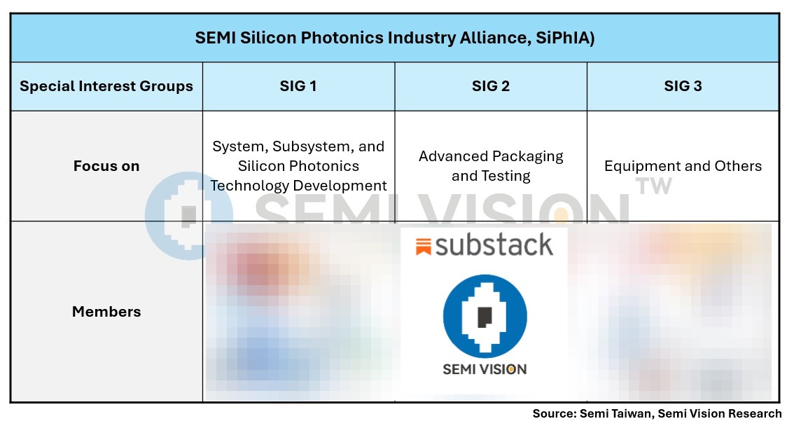
To address these challenges and accelerate breakthroughs and commercialization, the SEMI Photonics Consortium has established three SIGs with the following technical roadmaps:
SIG 1: Systems, Subsystems, and Silicon Photonics Technology Development
Focuses on future trends in silicon photonics, including chip design, manufacturing, and integration, aiming to build a comprehensive silicon photonics ecosystem.
Dr. Wei-Chung Lo, Deputy Director of the Electronic and Optoelectronic System Research Laboratories at ITRI, noted that the silicon photonics technology roadmap is steadily advancing from 100G and 200G to 400G transmission speeds. Each generation adopts different specification architectures, with “pluggable modules” currently being the most commonly used approach.
SIG 2: Advanced Packaging and Testing
Concentrates on heterogeneous integration, co-packaged optics (CPO), and testing technologies that drive the convergence of optics and electronics.
The two major current challenges are “optical coupling” and “testing.”
SIG 3: Equipment and Others
Dedicated to developing and providing critical tools and technologies for the silicon photonics industry, with a focus on process automation, assembly, inspection, and innovative equipment solutions.
Building upon the technology roadmap of SIG 1 and the packaging and testing focus of SIG 2, SIG 3 is tasked with defining the necessary measurement equipment and materials.
SEMI Global Chief Marketing Officer and President of SEMI Taiwan, Terry Tsao, stated that the SEMI Photonics Consortium is centered on Taiwan’s semiconductor industry and unites over 110 leading domestic and international companies. It has become the world’s largest and most comprehensive international platform for technical collaboration in silicon photonics. The consortium spans the entire supply chain—from upstream to downstream—and integrates cross-company and cross-disciplinary resources to fuel global innovation. With the official launch of the three SIGs, the alliance will promote breakthroughs in critical technologies, accelerate the standardization process, and tackle the challenge of fragmented technology development.
Established in September 2024, the SEMI Photonics Industry Consortium is committed to advancing silicon photonics technology. The three SIGs collectively span the full industry value chain—from system design and device manufacturing to packaging and testing.
Forum Agenda
2:50 PM – 3:15 PM
Keynote: Recent Activities on Silicon Photonics for Datacom and Telecom
Dr. Shin Kamei, General Manager, NTT Innovative Devices
NTT has been actively advancing silicon photonics technologies to meet the growing demands of datacom and telecom applications. Their efforts focus on integrating photonic and electronic components to achieve high-speed, energy-efficient data transmission.
Key Initiatives:
• IOWN Initiative: NTT leads the Innovative Optical and Wireless Network (IOWN) initiative, aiming to develop an all-photonics network that offers ultra-low latency and high-capacity communication. This involves creating an end-to-end optical communication system, reducing reliance on electronic components to enhance performance and energy efficiency.
• Photonics-Electronics Convergence: NTT is exploring the convergence of photonics and electronics to overcome the limitations of traditional electronic systems. By integrating photonic technologies directly into computing and networking infrastructure, they aim to increase speed, reduce latency, and improve energy efficiency.
These initiatives position NTT at the forefront of silicon photonics development, contributing to the evolution of next-generation communication networks.
3:15 PM – 3:40 PM
Advancing CPO Technology with Multiphysics Design Solutions from Ansys
Dr. Yi-Hao Chen, Principal Application Engineer, Ansys
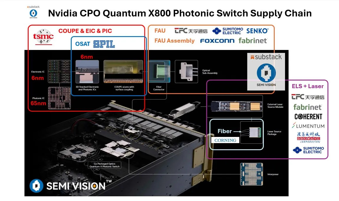
Ansys and TSMC have collaborated to advance Co-Packaged Optics (CPO) technology by integrating Ansys’ multiphysics simulation tools with TSMC’s Compact Universal Photonic Engines (COUPE) platform. This partnership addresses the increasing demands of high-speed, low-power data communication in applications such as artificial intelligence (AI), high-performance computing (HPC), and data centers.
Key Highlights:
• COUPE Platform: TSMC’s COUPE is a silicon photonics integration system designed to enhance chip-to-chip and machine-to-machine communication. It integrates multiple electrical integrated circuits (ICs) with photonic ICs and fiber optic connections into a single package, aiming to reduce coupling loss and improve performance.
• Ansys Multiphysics Solutions: Ansys provides a suite of simulation tools that support the design and analysis of COUPE-based systems:
• Ansys Lumerical™ for photonic simulation.
• Ansys Zemax™ for optical input/output simulation.
• Ansys RedHawk-SC™ and Ansys Totem™ for power integrity and thermal management.
• Ansys RaptorX™ for high-frequency electromagnetic analysis.
• Integration with Design Platforms: These Ansys tools are integrated with Synopsys’ 3DIC Compiler, facilitating a unified exploration-to-signoff platform that streamlines the design process for complex photonic and electronic systems.
This collaboration enables designers to tackle challenges associated with integrating photonic and electronic components, ensuring efficient thermal management, power integrity, and electromagnetic compatibility. By leveraging these combined technologies, the industry can accelerate the development of next-generation communication systems that are faster, more efficient, and capable of handling the growing demands of modern applications.
3:40 PM – 4:05 PM
Challenges of SiPh Assembly & Testing
ficonTEC
We will host dedicated discussions for our paid members, focusing on in-depth topics and exclusive insights.
4:05 PM – 4:30 PM
Shaping the Silicon Photonics Future through Opto-Mechatronics Integration
We will host dedicated discussions for our paid members, focusing on in-depth topics and exclusive insights.
4:30 PM – 4:55 PM
The Evolving Role of Optics in AI Clusters
Dr. Vladimir G. Kozlov, Founder and CEO, LightCounting
Dr. Vladimir G. Kozlov, Founder and CEO of LightCounting, has extensively discussed the evolving role of optics in AI clusters, emphasizing the critical need for high-bandwidth, low-latency optical interconnects to meet the demands of modern AI workloads. As AI models grow in complexity and scale, traditional electrical interconnects face limitations in bandwidth and energy efficiency.
Key Insights:
• Optical Interconnects for AI Clusters: Dr. Kozlov highlights the transition from electrical to optical interconnects in AI clusters to support the massive data exchange required between compute nodes. Optical solutions offer superior bandwidth and lower latency, essential for efficient AI processing.
• Power Efficiency: A significant challenge in scaling AI infrastructure is managing power consumption. Optical interconnects consume less power compared to their electrical counterparts, making them a more sustainable choice for large-scale AI deployments.
• Co-Packaged Optics (CPO): The integration of optics directly with processing units, known as Co-Packaged Optics, is identified as a key strategy to reduce energy consumption and improve performance in AI systems.
• Market Trends: Dr. Kozlov’s research includes detailed forecasts on the adoption of optical technologies in AI clusters, analyzing sales data of optical transceivers and projecting growth trends from 2021 to 2029.
These insights underscore the pivotal role of optical technologies in advancing AI infrastructure, addressing both performance and energy efficiency challenges.
If you would like to explore the silicon photonics roadmaps of TSMC and NVIDIA in greater depth, please refer to our previously published articles for more detailed analysis and insights.
For TSMC, silicon photonics is becoming a critical interconnection technology to support next-generation AI chips. One of TSMC’s key customers, NVIDIA, is continuously pushing the limits of chip-to-chip bandwidth, making optical transmission an inevitable trend. To address this, TSMC must integrate with Taiwan’s broader semiconductor supply chain to enable scalable photonic solutions.
We anticipate that Optical I/O will be a core component of NVIDIA’s upcoming Feynman architecture, enabling high-speed interconnects through optical links. Notably, NVIDIA has already incorporated silicon photonics into its Quantum X platform, which was showcased at GTC 2025.
For more details, please refer to our earlier article on this topic.