

Beyond Chips: Unveiling the Future of the Global Silicon Photonics Ecosystem
Original Article by SemiVision Research

SemiVision Research has released an updated version of the optical module supply chain analysis.


The new report primarily categorizes optical modules based on a scale-up and scale-out framework, and further classifies them by light source technologies, focusing on VCSEL, EML, and CW DFB lasers. From a packaging perspective, the modules are differentiated into LPO (Linear Pluggable Optics) and CPO (Co-Packaged Optics).
In addition, we also explore emerging areas in silicon photonics, such as Optical Couplers, EIC (Electronic Integrated Circuit) Testing, PIC (Photonic Integrated Circuit) Testing, Probers, Advanced Packaging for CPO, new innovations in materials, and OSP (Optical Signal Processors).
If you are a silicon photonics-related company that was not listed above, we warmly invite you to reach out to us.
Companies with innovative silicon photonics technologies are also welcome to contact us for potential collaboration opportunities.
E-mail : jett@semivisiontw.com
The report concludes with a comprehensive overview of the various players’ ecosystems across the industry.
If you would like to stay updated with the latest semiconductor industry insights, feel free to follow us on LinkedIn.
SemiVision Research: Global Silicon Photonics Supply Chain Analysis
Based on SemiVision Research’s current assessment of the global silicon photonics (SiPh) ecosystem, the supply chain can be systematically categorized into key stages as follows:
The fabrication of an optical engine is achieved through a series of crucial and precisely controlled manufacturing processes.
SOI Wafer Supply (Photonic SOI Substrates)
Scope: Supply of high-quality silicon-on-insulator (SOI) wafers specifically optimized for photonics (thicker device layers, low optical loss, uniformity control).
Key Materials: 220 nm SOI, 400 nm SOI, custom photonic SOI.
Critical Challenges:
Optical loss management (refractive index)
Thickness uniformity (Box Oxide)
Wafer defect density control for photonic-grade requirements
Key Speech in SOI Photonic wafer by Soitec

PIC Design and EDA Tools (Photonic Integrated Circuit Design)
Scope: Design and simulation of PICs (Photonic Integrated Circuits), requiring specialized EDA tools beyond traditional electronic design.
Core Tools:
Photonic layout (PCells, DRC/LVS for PIC)
Optical simulation (FDTD, BPM, Eigenmode solvers)
Critical Challenges:
Accurate co-design of PIC + EIC (Co-optimization)
Compact model libraries (CML) generation
Managing variability in optical performance post-fabrication


Photonic Foundry (SiPh Process Manufacturing)
Scope: Fabrication of photonic circuits using CMOS-compatible processes (Si, SiN, Ge-on-Si, III-V integration).
Service Models: Dedicated photonic foundry (Ayar Labs, CompoundTek), or multi-project wafer (MPW) service (e.g., TSMC SiPh service, IMEC).
Critical Challenges:
PIC-specific process modules (e.g., grating couplers, modulators)
Thermal tuning structures
Process design kit (PDK) maturity for optical device variants


Key Articles Related to the OFC 50 Forum:


EIC and DSP Design (Electronic Integrated Circuits & Digital Signal Processing)
Scope: Design of electronic circuits supporting optical functions (modulator drivers, transimpedance amplifiers (TIA), ADC/DACs, SerDes, DSP engines).
Critical Challenges:
Co-design for bandwidth, noise, linearity
Power efficiency optimization for SerDes and DSP blocks
Light Source (Laser Supply and Integration)
Scope: Provision of lasers used for optical transmission (on-chip laser integration vs. external laser source feeding).
Types:
DFB, EML, Quantum Dot Lasers (Quintessent , QD Laser Inc ,Innolume GmbH,Nanoco Technologies Ltd,Nanosys Inc.,Cybel LLC)
External C-Band and O-Band lasers for DWDM systems
Critical Challenges:
Thermal management of integrated lasers
Laser packaging yield and coupling efficiency
ELSFP and Optical Interfaces
Scope: Development of advanced pluggable or embedded optical modules, such as ELSFP (Extended Linear Small Form-factor Pluggable).
Purpose: Bridge between optical engines and external cabling systems.
Critical Challenges:
Managing power consumption at >400G/800G/1.6T rates
Connector thermal design and mechanical stability
Optical Fiber and Connector Supply
Scope: Supply of high-specification fibers and advanced optical connectors for coupling to PICs.
Types:
Single-mode fiber (SMF), polarization-maintaining fiber (PMF)
Specialized connector designs (MT ferrule, Angled-Polished Connectors (APC))
Critical Challenges:
Precision fiber array manufacturing
Fiber attachment reliability
Loss management across fiber/PIC interfaces
Optical Engine Assembly (Co-Packaging and Integration)
Scope: Full integration of PICs, EICs, lasers, fiber arrays into a single optical engine or CPO (Co-Packaged Optics) module.
Critical Challenges:
Active alignment of fiber to waveguide
Thermal management
Mechanical robustness under thermal cycling and operational stress

PIC and EIC Testing (Wafer Level Testing and Final Testing)
Scope: Electrical, optical, and optoelectronic characterization at wafer, die, and package level.
Critical Challenges:
Dual-sided wafer testing (Double side)
Optical port testing automation (In sequence testing solution)
Minimizing handling-induced yield loss ( CP + WAT + FT + ATE )


Optical Coupler Development (Waveguide Couplers)
Scope: Development of low-loss optical couplers to connect fiber to PICs efficiently.
Types:
Surface grating couplers
Edge couplers
Vertical couplers
Critical Challenges:
Insertion loss optimization
Polarization sensitivity management
Alignment tolerance improvement


UV Resin and Bonding Materials
Scope: Specialized UV-cured adhesives and bonding resins for optical fiber attachment, PIC encapsulation, or laser bonding.
Representative Suppliers: DELO, Dymax
Critical Challenges:
Optical transparency
Low shrinkage and thermal stability
Long-term reliability under operation (temperature cycling, humidity)
Overall Key Challenges Silicon Photonics Faces at System Level
End-to-end optical alignment precision
Wafer-level optical testing throughput
Co-design between optics and electronics
Laser integration complexity (on-chip vs. external)
Packaging-induced thermal stress management
Industrial-grade manufacturing repeatability and scalability

Following the completion of the optical engine, the manufacturing process proceeds to the CoWoS integration stage, where the GPU and HBM are bonded onto the interposer. SemiVision has compiled a detailed analysis of the CoWoS and HBM materials and equipment supply chain.
From the image, it is evident that over 90% of the backend packaging materials are dominated by Japanese companies! The proportion is very high!
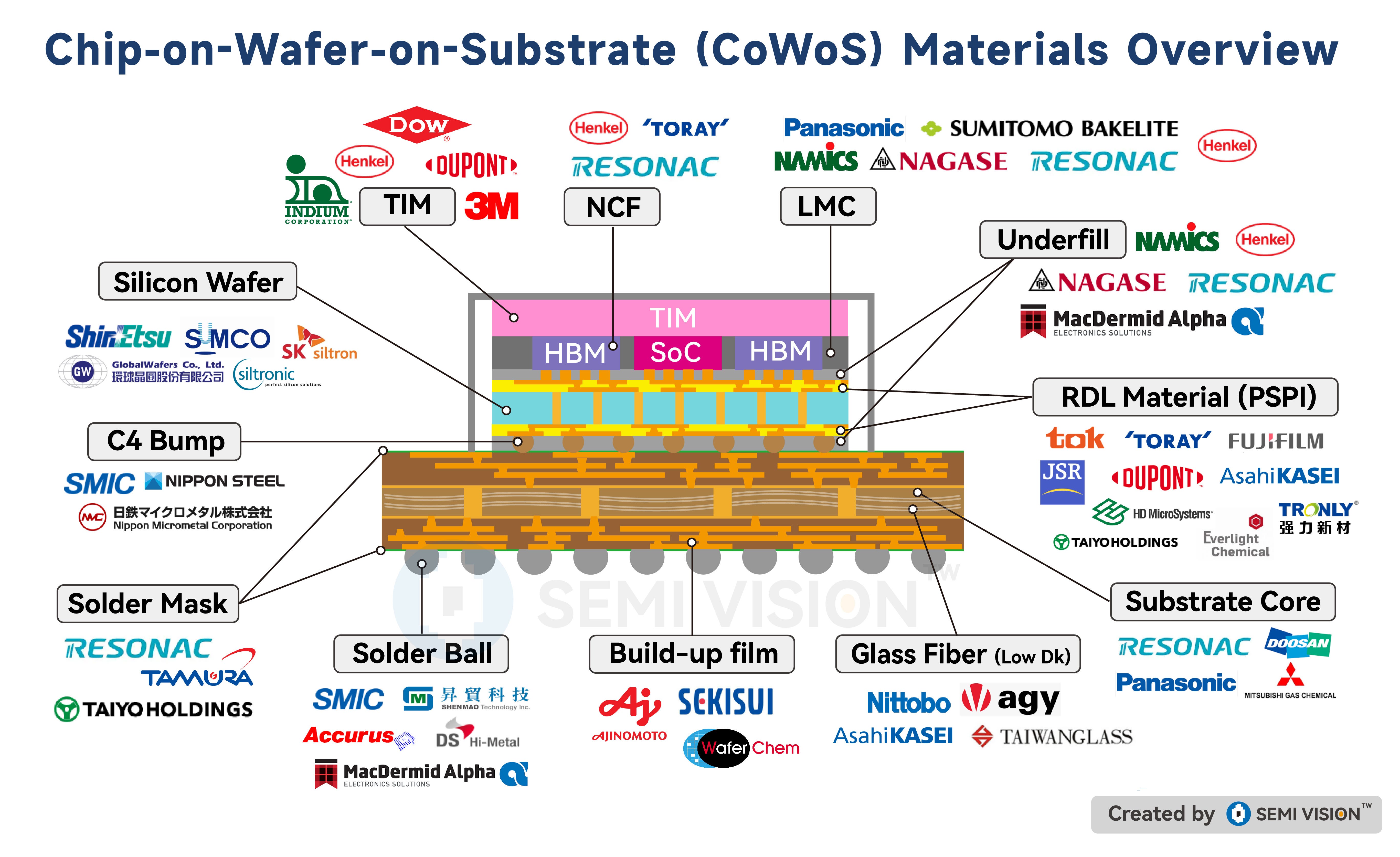
However, currently, TSMC's CoWoS capacity is continuously increasing, but some Japanese material manufacturers are unable to keep up with the demand. It is understood that shortages have already emerged for several key materials, and major AI chip companies are starting to require OSATs/substrate manufactuer to prepare a second source in advance to meet future capacity needs.
SemiVision , our previous analysis of the CoWoS material supply chain received widespread praise. This time, we are focusing on the highly discussed topic of HBM (High Bandwidth Memory) under the context of U.S.-China export restrictions.
Key Focus on HBM Regulations:
Based on the importance of HBM described above, Bureau of Industry and Security (BIS) is adding a new ECCN control on HBM stacks with a specific memory bandwidth density to ECCN 3A090.c. BIS uses the bandwidth density—rather than just the bandwidth—to ensure controls will still apply if an IC uses a larger quantity of smaller HBM chips at little additional cost. Under new 3A090.c, this IFR will control HBM having a ‘memory bandwidth density’ greater than 2GB per second per square millimeter (mm). All HBM stacks currently in production exceed this threshold.
Regarding the recent 3A090.c technical note, it specifies that certain co-packaged integrated circuits are excluded from the scope of 3A090.c. These exclusions apply to co-packaged ICs with both HBM and logic, where the primary function of the IC is processing. However, the note also clarifies that the control does cover HBM permanently affixed to a logic IC designed as a control interface with a physical layer (PHY) function.
Thus, our attention shifts to the HBM base die design—a critical yet complex area of the HBM industry that encompasses materials, equipment, advanced packaging, and advanced HBM IP.
Analysis Areas:
In this analysis, we will focus on the following supply chain elements:
• Silicon wafer
• Molding process
• TCB (Thermo-Compression Bonding) process
• Hybrid bonding
• Dicing/Grinding
• CMP (Chemical Mechanical Polishing)
• HBM IP
Notable Observations:
1. TSMC has adopted 12nm and 5nm advanced logic technologies for applications in the HBM domain.
2. Companies like Marvell and Broadcom have introduced their advanced packaging platforms, integrating custom HBM solutions.
3. Looking ahead, HBM3E will evolve into HBM4 in the next generation, with anticipated changes. Furthermore, HBM5 is expected to incorporate new 3D SiP (System-in-Package) concepts.
Future Focus:
For the AI sector, we must emphasize two key areas:
1. HBM advancements.
2. Silicon photonics integration.
If any of the above topics interest you, feel free to reach out for further discussion!
SemiVision has provided a brief overview of key components within the silicon photonics domain.
1. PIC Design (Photonic Integrated Circuit)
PIC design (Photonic Integrated Circuit) refers to the technology of integrating multiple optical components—such as lasers, modulators, waveguides, optical switches, and photodetectors—onto a single chip. The goal is to enable high-speed, low-power, and high-density optical signal processing and transmission. Similar to traditional electronic IC design, PIC design must consider the arrangement of components, dimensions, functional modularization, signal integrity, thermal management, and integration with electronic circuits (EIC).
Silicon photonics is currently the most dominant PIC platform, leveraging mature CMOS manufacturing processes to achieve cost-effective, high-volume integration of photonic and electronic devices. The design workflow typically includes system-level modeling (using tools like VPI or Lumerical for simulation), parameter optimization of subcomponents (such as Mach-Zehnder modulators or ring resonators), layout design (using PDA tools like Synopsys OptoCompiler), Process Design Kit (PDK) matching, and EDA verification processes.
Since optical wavelengths are much larger than the feature sizes in electronic components, PIC design must carefully address layout density, waveguide bending loss, coupling efficiency, and multimode interference. Additionally, temperature drift effects on component performance must be managed. Overall, PIC design is evolving toward higher integration levels, smaller chip footprints, and heterogeneous integration (such as III-V on Silicon or InP and Ge detectors) to support applications in AI, data centers, high-bandwidth interconnects, and sensing.
This trend creates both opportunities and challenges. Opportunities include high-potential applications in emerging fields like 400G/800G optical communications, quantum photonics, photonic AI accelerators, and automotive LiDAR, as well as strong demand for heterogeneous integration EDA tools and IP modules. Challenges include the immaturity of design tools and component models, difficulty in yield prediction, lack of standardized testing methods, and technical barriers in co-packaging and thermal management with electronic circuits. As the industry moves toward the chiplet era, modularity, reusability, and compatibility with advanced packaging platforms will become critical competitive advantages.
Key Companies Providing PIC Design and Development Services
VLC Photonics: Offers design services across a wide range of material platforms, including SOI (Silicon on Insulator), SiN (Silicon Nitride), InP (Indium Phosphide), and TFLN (Thin-Film Lithium Niobate).
VLC Photonics, based in Valencia, Spain, is a Photonic Integrated Circuit (PIC) design and testing company founded in 2011 as a spin-off from the Polytechnic University of Valencia.
The company specializes in providing end-to-end PIC development services, covering consulting, design, fabrication, testing, and packaging across various material platforms, including Silicon Photonics, Indium Phosphide (InP), Silicon Nitride (SiN), PLC, and polymers.
In November 2020, VLC Photonics was acquired by Hitachi High-Tech, further strengthening Hitachi’s capabilities in the photonics sector.
Bright Photonics: Specializes in PIC design based on silicon and III-V compound semiconductor materials.
Bright Photonics, located in Eindhoven, the Netherlands, is an independent PIC design company founded in 2010.
The company provides comprehensive PIC development services from initial concept and prototyping to mass production design.
Its services span multiple material platforms, including Silicon, III-V semiconductors, Silicon Nitride (SiN), Silica, and polymers.
Spark Photonics: Provides end-to-end PIC design services, covering multiple material platforms.
Spark Photonics, based in Waltham, Massachusetts, USA, specializes in PIC design services and educational initiatives.
Founded in 2019 by Dr. Kevin McComber, the company is structured into two main divisions, offering design services across various material platforms.
SiFotonics: Focuses on rapid prototyping of silicon photonic integrated circuits.
SiFotonics Technologies Co., Ltd. is a fabless semiconductor company specializing in Silicon Photonics devices and integrated circuits.
Founded in 2007 and headquartered in Woburn, Massachusetts, USA, the company also maintains offices in Beijing, Shanghai, Nanjing, Hsinchu (Taiwan), Hong Kong, and San Jose (California).
NewPhotonics: Focuses on developing next-generation silicon photonic integration platforms, aiming for higher bandwidth density and heterogeneous integration with advanced materials.
NewPhotonics, headquartered in Tel Aviv, Israel, is a fabless semiconductor company established in 2020.
It specializes in developing Photonic Integrated Circuits (PICs) for next-generation data centers in the AI era, aiming to enable full optical interconnects to reduce latency and power consumption while meeting the demands of high-performance computing and AI workloads.
Lightwave Logic: Specializes in polymer-based photonic devices, developing ultra-high-speed optical modulators using proprietary electro-optic polymers for future optical interconnect and communication applications.
Lightwave Logic, based in Englewood, Colorado, USA, is a technology platform company dedicated to developing next-generation electro-optic (EO) polymer materials and photonic devices.
Its core technologies aim to enhance data transmission speeds in data centers and telecom networks while reducing power consumption, meeting the increasing demand for high-speed, low-latency connectivity driven by Generative AI and high-performance computing.
2. EIC Design (Electronic Integrated Circuit)
EIC design (Electronic Integrated Circuit) focuses on the development of electronic circuits for driving, control, and signal processing, playing a crucial role in silicon photonics or photonic integrated circuit (PIC) systems. These circuits typically include laser drivers, modulator drivers (such as MZM drivers), transimpedance amplifiers (TIAs), clock and data recovery circuits (CDRs), serializers/deserializers (SerDes), and ADC/DAC components. Their function is to provide the necessary driving voltages and currents to convert electronic signals into optical signals, or to convert received optical signals back into processable electronic data.
EIC design must balance high-frequency response, low noise, high linearity, and low power consumption, while also addressing reliability and thermal stability challenges at advanced process nodes such as 16nm or 7nm. Common technology platforms include CMOS, BiCMOS, and SiGe processes. Among them, BiCMOS and SiGe are better suited for high-speed analog signal processing but come with higher costs and greater process complexity.
The integration of EIC and PIC is becoming increasingly important, particularly in applications such as CPO (Co-Packaged Optics), LPO (Linear Drive Pluggable Optics), and OIO (Optical I/O). Key design challenges include achieving dense packaging within limited space, maintaining signal integrity, and controlling thermal effects.
At the same time, opportunities for EIC design are expanding rapidly. As optical modules evolve toward 400G, 800G, and even 1.6T speeds, demand for high-line-rate drivers and low-noise receivers is surging. Furthermore, the widespread adoption of AI, high-performance computing (HPC), and edge devices places higher demands on EIC capabilities for high bandwidth, low latency, and low power consumption. This is also accelerating innovation in EDA tools, IP libraries, and heterogeneous integration technologies.
In the future, companies that can integrate EIC design, packaging, and testing with PICs will become key platform players in the era of optoelectronic heterogeneous integration.
Leading companies in high-performance EIC design include:
Intel: Actively applying its advanced EIC technologies to the silicon photonics field.
Broadcom: A leader in designing high-speed SerDes, TIAs, and drivers for optical applications.
NVIDIA: Expanding its expertise in high-performance EICs into silicon photonics, particularly for AI and HPC infrastructure.
3. EDA Tools (Electronic Design Automation)
EDA tools (Electronic Design Automation) are comprehensive software toolchains that support the development of electronic and optoelectronic integrated circuits, covering system modeling, device design, circuit simulation, layout generation, verification, and production readiness. They are critical to the development of modern electronic and silicon photonics systems.
In traditional EIC design, EDA tools such as Cadence, Synopsys, and Mentor (now Siemens EDA) have established highly mature design workflows, including front-end RTL design and synthesis, analog/mixed-signal simulation, timing analysis, DRC/LVS verification, and physical layout implementation.
In the field of silicon photonics and photonic integrated circuits (PICs), however, EDA tools are undergoing transformation and integration challenges. They must now support complex optical behavior modeling, coupling loss simulation, optical waveguide design, and Process Design Kit (PDK) management. Leading photonic EDA platforms such as Synopsys OptoCompiler, Ansys Lumerical, Luceda IPKISS, and VPIphotonics are gradually integrating with electronic design workflows, promoting electro-optical co-design methodologies.
Moreover, as next-generation optical modules such as CPO (Co-Packaged Optics), LPO (Linear Drive Pluggable Optics), and OIO (Optical I/O) move toward highly heterogeneous integration and modular packaging, EDA tools must also incorporate packaging simulation (e.g., Ansys Icepak, HFSS), signal and power integrity (SI/PI) analysis, optothermal coupling modeling, and multiphysics verification capabilities.
This shift creates significant opportunities, especially in the AI HPC and optoelectronic SoC domains, where a unified EDA platform is urgently needed to support end-to-end collaboration from chip design to packaging and testing. However, the challenges are also considerable, including the lack of unified standards for heterogeneous optoelectronic integration, inconsistent accuracy of photonic PDKs and device models, and a general lack of modularity and reusability in design flows. Overcoming these hurdles will require cross-industry collaboration and support from open-source communities.
In the future, EDA tools will not merely serve as design aids but will become foundational pillars determining whether large-scale deployment of heterogeneous integration and electro-optical co-design can be achieved.
Key players and platforms include:
Synopsys OptoCompiler: A unified platform combining electronic and photonic design capabilities.
Cadence EPDA: Provides design workflows supporting both monolithic and heterogeneous integration.
Luceda Photonics: Specializes in professional photonic IC design software and services.
Siemens EDA: Offers a comprehensive resource library for photonic design solutions.
4. Foundry Manufacturing
Foundry manufacturing refers to semiconductor fabrication services that specialize in transforming IC design files (such as GDSII or OASIS) from fabless companies into physical chips. Foundries play a central role in both electronic integrated circuit (EIC) and photonic integrated circuit (PIC) industries.
For silicon photonics and heterogeneous integration applications, foundries must not only possess conventional CMOS process capabilities but also support technologies such as optical waveguide fabrication, optical modulators, photodetectors, and even heterogeneous integration of III-V laser materials.
Today’s leading foundries providing silicon photonics manufacturing include:
TSMC
GlobalFoundries
Intel Foundry Services
Tower Semiconductor
IMEC (European research-based foundry)
SMART Photonics (specializing in InP platforms)
Ligentec (focusing on SiN platforms)
CompoundTek (a Singapore-based dedicated silicon photonics foundry)
These foundries differ in their supported waveguide materials (e.g., Si, SiN, InP), process nodes, and the maturity of their Process Design Kit (PDK) offerings. The value of a foundry lies not only in manufacturing but also in providing reusable design platforms (PDKs), Multi-Project Wafer (MPW) services, and scalable paths to volume production—allowing startups and research institutions to prototype and iterate photonic and electronic components more cost-effectively.
Current challenges in silicon photonics manufacturing include controlling photonic device yields, stabilizing coupling efficiency, ensuring material thermal stability during high-temperature processing, and addressing thermal expansion mismatch and bonding yield issues in highly heterogeneous integration processes (e.g., III-V on Silicon or CMOS-Photonic co-packaging). Additionally, photonic devices are more sensitive to geometric imperfections compared to traditional CMOS devices (e.g., sidewall roughness causing scattering loss), requiring foundries to invest heavily in etching precision, deposition quality, mask accuracy, and metrology technologies.
On the opportunity side, the explosive growth of generative AI and data center markets is driving massive demand for high-bandwidth, low-power optical interconnects, opening up significant investment opportunities for foundries. Expanding process capabilities to support platforms such as CPO (Co-Packaged Optics), LPO (Linear Drive Pluggable Optics), and OIO (Optical I/O) will position foundries as critical infrastructure providers for the next generation of high-speed optical communications.
Foundries that can support electronic-photonic heterogeneous integration, offer standardized PDKs, and establish a full-stack ecosystem for mass production will occupy key positions in the AI and HPC optical communication supply chain.
Key foundries include:
TSMC: Offers a full-service platform covering PIC, EIC, and 3D integrated packaging solutions.
GlobalFoundries: Provides the GF Fotonix™ platform, enabling high-performance silicon photonics manufacturing.
Tower Semiconductor: Operates a high-capacity silicon photonics manufacturing platform.
AIM Photonics: Delivers comprehensive services including design, simulation, manufacturing, and packaging.
5. Hybrid Bonding
Hybrid bonding is a high-density heterogeneous integration packaging technology that enables extremely high I/O density, low-latency, and high-bandwidth signal interconnects between chips (chip-to-chip) or between chips and wafers (chip-to-wafer / wafer-to-wafer). It is a core technology driving 3D ICs, optoelectronic integration (such as CPO), and advanced packaging architectures like TSMC SoIC and Intel Foveros.
Unlike traditional thermal compression or metal bump bonding methods (such as micro-bumps or Cu-pillars), hybrid bonding combines oxide-to-oxide bonding (after chemical-mechanical polishing) with direct copper-to-copper (Cu-Cu) metal contact. This approach enables nanometer-level alignment precision, ultra-small pitches (currently below 10μm), and ultra-low resistance electrical connections, significantly enhancing interconnect performance and system integration density.
For silicon photonics applications, hybrid bonding allows photonic integrated circuits (PICs) and electronic integrated circuits (EICs) to be interconnected at extremely short distances, achieving true co-packaged electro-optical integration. It also enables high-bandwidth photonic subsystem coupling in multi-chip modules, such as CPO switches, photonic AI processors, or high-efficiency laser array coupling onto silicon photonic chips.
The main challenges include achieving ultra-precise alignment (especially for coupling optical waveguides and photodetectors), maintaining a clean process environment (to avoid oxidation contamination and void formation), addressing reliability issues caused by thermal expansion coefficient mismatches, and ensuring defect detection during testing and mass production (currently relying on a combination of AOI and X-ray inspection). These challenges demand highly mature process controls and equipment integration.
On the opportunity side, as AI computational power consumption rises and the memory wall bottleneck worsens, hybrid bonding offers a crucial solution to improve system performance density. It shows tremendous potential in chiplet architectures, 3D packaged memories, and the stacking of photonic chips with laser arrays. Leading companies and organizations, including TSMC, Intel, Amkor, ASE, and Yole Développement, have identified hybrid bonding as a foundational technology for the next decade of advanced packaging.
Suppliers specializing in hybrid bonding solutions include:
EV Group (EVG): Offers wafer-to-wafer hybrid bonding technologies.
SUSS MicroTec: Provides the XBS300 platform, supporting 200mm and 300mm wafer hybrid bonding.
Applied Materials: Delivers advanced hybrid bonding solutions, including the Insepra™ SiCN and Catalyst CMP systems.
ASMPT: Introduced the LITHOBOLT™ platform to meet the demands of next-generation semiconductor packaging.
6. Optical Coupler
An optical coupler is a critical component in silicon photonics and optical communication systems, responsible for directing optical signals into and out of photonic integrated circuits (PICs). Its primary function is to precisely couple light from external sources (such as lasers) into on-chip optical waveguides or to extract optical signals from waveguides for transmission, detection, or conversion.
Depending on the coupling direction and application, optical couplers can be categorized into fiber-to-chip, laser-to-chip, and chip-to-chip types. Common coupling technologies include grating couplers and edge couplers. Grating couplers utilize nano-periodic surface structures to convert vertically incident light into guided modes, facilitating mass production and automated alignment but with relatively limited efficiency and bandwidth. Edge couplers, on the other hand, directly couple horizontally between waveguide facets and fibers, achieving higher coupling efficiency and bandwidth, making them ideal for high-performance applications, though they require extremely precise alignment and high-quality wafer cleaving.
In high-speed optical modules, CPO (Co-Packaged Optics), LPO (Linear Drive Pluggable Optics), and photonic AI processors, optical couplers play an increasingly critical role. Parameters such as coupling efficiency, insertion loss, return loss, alignment tolerance, and thermal stability directly impact overall module performance and cost.
Challenges in coupler design and manufacturing include bridging the size mismatch between waveguides and fiber cores, mitigating efficiency variation caused by nanoscale fabrication errors, and maintaining alignment yield and repeatability during mass production. In multi-wavelength applications (such as DWDM), couplers must support broadband or wavelength-selective structures, further complicating design and fabrication.
On the opportunity side, the rise of heterogeneous electro-optical integration and the need for higher bandwidth are accelerating the development of new coupling solutions, such as 3D micro-lenses, metasurface-based optical antennas, hybrid polymer bonding, vertical coupling from VCSEL to waveguide, and glass waveguide intermediaries. High-efficiency, low-cost, large-alignment-tolerance couplers compatible with CMOS processes are positioned to become the critical enabler for scaling silicon photonics and advanced optical module production. They will also serve as a key driver for innovation in the broader optical communications and AI hardware architecture landscape.
Key companies providing advanced coupler solutions include:
Teramount: Offers the Universal Photonic Coupler, enabling high-density optical fiber-to-silicon photonic chip connections.
Chiral Photonics: Provides optoelectronic coupling and packaging services, including both electrical and optical I/O solutions.
7. Assembly & Packaging
Assembly and packaging are critical processes in electronic and optoelectronic systems, responsible for integrating chips (dies) into modules or system-in-package (SiP) formats, while completing the necessary electrical, optical, thermal, and mechanical connections. In silicon photonics (Silicon Photonics) and photonic integrated circuits (PICs), assembly and packaging play an indispensable role.
Unlike pure electronic IC packaging, photonic module assembly and packaging involve complex interactions across optics, electronics, thermals, mechanics, and materials. Key requirements include precise coupling of fibers or lasers, alignment of optoelectronic components, high-frequency electrical interconnections, thermal path optimization, and mechanical protection of modules. Typical optical-electrical packaging processes involve die attach, fiber/laser/detector alignment and coupling, optical adhesive bonding, wire bonding or bump bonding, sealing, testing, and reliability verification. These processes heavily rely on high-precision automated equipment and active/passive alignment technologies, such as sub-micron bonding machines and vision-based alignment systems.
In the context of 800G/1.6T high-speed optical modules, CPO (Co-Packaged Optics), OIO (Optical I/O), and photonic AI processors, traditional OSAT (Outsourced Semiconductor Assembly and Test) providers—such as ASE, Amkor, and JCET—along with emerging photonic packaging companies like ficonTEC, AIT, and TFLux, are actively developing silicon photonics packaging solutions.
On the opportunity side, the future of optical modules is shifting toward external laser source (ELS) architectures and CPO structures, driving packaging demands from single-chip to multi-chip heterogeneous integration. There is an increasing need to achieve low-loss optical coupling and high I/O density within extremely compact volumes. This trend creates new opportunities for advanced packaging technologies such as glass substrates, RDL interconnects, chiplet hybrid bonding, fiber arrays, and meta-lenses.
However, optical-electronic packaging also faces substantial challenges, including maintaining coupling efficiency and repeatability, scaling coupling alignment to high-throughput manufacturing with good yield, ensuring high-frequency signal integrity, guaranteeing the thermal and moisture stability of optical adhesives and packaging materials, and significantly reducing packaging and testing costs. Overcoming these challenges requires cross-disciplinary innovation integrating equipment, materials, design, and process technologies.
Platforms capable of achieving high-precision automated optical packaging, supporting CPO and PIC-EIC integration, and enabling mass production will become essential pillars for the future architectures of AI, HPC, and high-speed data centers.
Key companies providing photonic assembly and packaging services include:
ASE (Advanced Semiconductor Engineering): Offers a comprehensive silicon photonics packaging platform, supporting high-density electro-optical interconnects and advanced packaging technologies.
PHIX Photonics Assembly: Provides PIC assembly and packaging services from prototyping to volume production.
ficonTEC: Specializes in high-precision automated photonic device assembly and testing solutions.
LioniX International: Offers PIC packaging and assembly services across various development stages.
8. Optical Modules
Optical modules are critical functional units in optical communication systems, responsible for converting electrical signals into optical signals (Tx, transmitter side) for transmission over fiber optics, and then converting optical signals back into electrical signals (Rx, receiver side) at the receiving end. They are widely used in data centers, telecommunications networks, AI supercomputers, high-frequency trading, and edge computing environments.
The core structure of optical modules typically includes an external laser source, modulators (such as MZM, EAM), optical waveguides, optical amplifiers, photodetectors (such as Ge PDs, InGaAs PDs), driver circuits, transimpedance amplifiers (TIAs), thermal management systems, and optical coupling interfaces (such as MT fiber arrays, grating couplers, or edge couplers). Module design must simultaneously address high bandwidth, low power consumption, low latency, high reliability, and miniaturization.
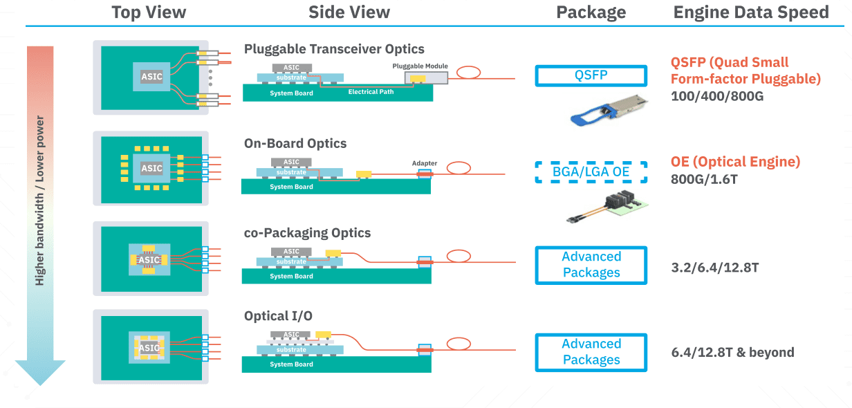
Optical modules can be categorized based on packaging format and interface standards, including:
Pluggable Modules (e.g., QSFP-DD, OSFP)
Linear-Drive Pluggable Optics (LPO)
Co-Packaged Optics (CPO)
Optical I/O Modules (OIO)
For example, 800G and 1.6T modules often adopt PAM4 modulation and integrate DSP, CMOS SerDes, or move towards DSP-free (LPO) or co-packaged (CPO) designs to achieve better energy efficiency (measured in pJ/bit).
Leading companies such as II-VI (now Coherent), Broadcom, Innolight, Accelink, Cisco Acacia, Intel, NVIDIA (through acquisitions), and Marvell (partnered with InnoLight) offer comprehensive portfolios of high-speed optical modules.
Challenges and Opportunities
Optical modules face significant challenges:
Bandwidth and power consumption limits (especially at 1.6T and future 3.2T)
Laser thermal stability and lifespan
Consistency in modulator and detector packaging
Coupling efficiency and automated assembly yields
Standardization and system compatibility issues
For example, under CPO and LPO architectures, traditional DSP-centric module designs are evolving toward analog-driven, low-latency control logic, raising requirements for electro-optical co-design and PIC/EIC co-packaging.
Opportunities are booming with the explosion of AI model inference and training demands. Hyperscalers (such as Google, AWS, Microsoft, and Meta) are aggressively opticalizing their internal data center architectures, driving massive demand for short-reach, high-speed modules (e.g., DR4/2xFR4, SR, LR).
Emerging technologies such as:
Photonic computing
Chip-to-chip optical interconnects
Glass waveguide integration
Meta-optical components
External laser sharing architectures (ELSFP)
Modular silicon photonics platforms (e.g., Intel’s LightBar, Ayar Labs’ TeraPHY)
are reshaping the optical module ecosystem, providing new opportunities for innovation.
The Evolution of Optical Modules
Traditional pluggable optical modules successfully drove data centers from 10G and 25G to 100G and 400G over the past decade. However, for 800G, 1.6T, and beyond, they are reaching limits in terms of power consumption, latency, bandwidth density, and thermal design. This is catalyzing a major architectural shift toward LPO (Linear Pluggable Optics) and CPO (Co-Packaged Optics).
Future optical modules will no longer merely serve as replaceable communication interfaces. Instead, they will become deeply integrated computing-network cores. Their design logic is shifting from “external modules” to “embedded computing units,” from “simple signal conversion” to “deep collaborative computation.” Key optical components—Tx/Rx units, drivers, waveguides, lasers, and photodetectors—will be restructured as Photonic Engines, photonic subsystems, and tightly integrated packages alongside AI accelerators, GPUs, or switch ASICs.
CPO epitomizes this transformation: by integrating photonic modules directly with switch ASICs or AI accelerators at the packaging level, it drastically shortens SerDes distances, resolves I/O bottlenecks, improves energy efficiency, and delivers terabit-scale throughput within a single package to meet the extreme demands of AI and generative models.
Impact on the Optical Module Supply Chain
To make CPO mainstream, the entire optical module supply chain must transform:
From Finished Modules to Subsystem Suppliers: Companies must evolve to offer fully integrated solutions, including PICs, EICs, optical submodules, meta-lens arrays, fiber arrays, and advanced packaging designs.
External Laser Source Adoption: Moving lasers outside the module body (ELS architecture) reduces thermal design pressures and improves reliability, creating new demands for coupling and packaging technologies.
Automated High-Precision Alignment and Hybrid Bonding: Technologies such as hybrid bonding, glass intermediary layers, and chiplet-based modular packaging will become critical to entering the CPO era.
Traditional module form factors like QSFP-DD and OSFP will gradually decline in importance. Future winners will be those mastering photonic-electronic heterogeneous integration, platformized design, and full-stack system integration.
Industry Examples
Chinese module leaders such as InnoLight, Accelink, and Eoptolink are showcasing 800G/1.6T LPO and CPO prototypes, building their own silicon photonics platforms and investing in automated photonic packaging.
International players like Intel, NVIDIA, Broadcom, and Marvell are expanding vertically by developing or acquiring co-packaged optics capabilities, aiming to deliver full-stack solutions from switches to modules for AI HPC architectures.
In this trend, the core of optical modules will shift from “speed” and “form factor” to “integration capability,” “platformization” and “heterogeneous collaboration.” Only those companies that master end-to-end integration—designing optical-electronic chips, packaging them at high precision, and scaling to volume production—will lead the next wave of AI network optical communications.
For Paid Members, SemiVision will provide full table in this article.
