Beyond TIM: Microchannel Architectures for Advanced Thermal Management
Original Articles By SemiVision Research (IEEE ECTC , KLA , EVGroup , Meta , TSMC ,HP , Google , ASE , SEMI )

In our previous discussions, we explored how MEMS technology can be leveraged to address thermal management challenges through the implementation of microchannel cooling. Building upon that foundation, this article delves into the fabrication of microchannels using MEMS-based semiconductor processes. We will further examine how bonding technologies—such as wafer-to-wafer (W2W) or die-to-wafer (D2W) bonding—enable the integration of device wafers, HBM (High Bandwidth Memory) wafers, and embedded microchannel structures. Through this analysis, we aim to illustrate how these advanced techniques can enable next-generation 3D-stacked architectures with enhanced thermal efficiency.


In the era of AI and high-performance computing (HPC), chip design is pushing the limits of power density and thermal load. As a result, thermal management has become the foremost concern in chip development. This is not merely a system-level engineering issue—it is a comprehensive challenge spanning chip architecture, process design, packaging, and system integration. In AI chips, we are not only dealing with extreme computational intensity but also facing a fundamental physical constraint: there are only three ways to transfer heat—conduction, convection, and radiation.
To begin with, modern AI chips are inherently “hot” designs—power densities often exceed hundreds of watts per square centimeter. These levels far surpass the capabilities of conventional server cooling techniques, making advanced cooling solutions such as cold plates and microchannel cooling essential.
However, despite the high power demands, our options for heat transfer remain limited. Thermal radiation is practically ineffective at room temperature—it increases with the fourth power of temperature (T⁴), and at standard operating conditions, its contribution to heat dissipation is negligible. Therefore, only thermal conduction and thermal convection are realistically viable for cooling AI chips.
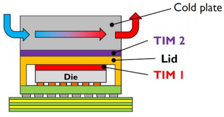
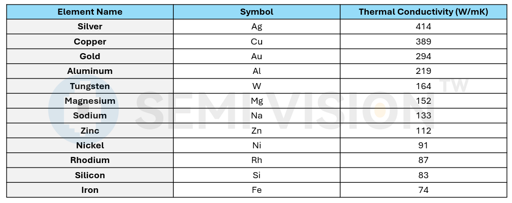
Thermal conduction governs how heat is extracted from within the chip. This heat path involves: the silicon substrate itself, metal interconnects, TIM1 (typically made of indium or graphite), the package lid, then TIM2 (such as graphite sheets or thin thermal pastes), and finally the heatsink or cold plate. Each layer’s thickness and thermal conductivity determines the efficiency of heat flow. For instance, TIM1 may be 100 microns thick, while TIM2 can be as thin as 1 micron—this design difference reflects the need to minimize thermal resistance (TR) and temperature gradients.
Thermal convection, on the other hand, deals with how quickly that heat is removed once it exits the chip package. From conventional fans and air cooling, to advanced cold plates and liquid cooling loops, to next-generation microchannel-based liquid cooling, system-level convection mechanisms have become essential to AI server infrastructure.
Within this framework, foundries and assembly houses must collaborate closely in thermal design. Traditionally, wafer fabrication and packaging were treated as separate domains, with boundaries defined by I/O and mechanical interfaces. But in the high-heat AI chip era, thermal design must transcend these boundaries. Wafer design must include provisions for thermal vias (TSVs) or copper pillars, backside trenches, and thermal spreaders. On the packaging side, one must integrate high-performance TIMs, optimized lid structures, microfluidic cold plates, and reliable fluidic interfaces. Packaging is no longer just about protection and I/O—it has become a core thermal management component.
This becomes even more critical with the increasing adoption of silicon photonics, which is highly temperature-sensitive. Minor thermal fluctuations—just a few tens of degrees—can cause optical drift, coupling losses, or complete failure. Traditional thermal design approaches are insufficient to meet these demands, requiring more proactive, localized, and fast-responding cooling strategies.
In summary, thermal design for AI chips is no longer a secondary step in the engineering flow. It is a multi-layered, interdisciplinary challenge that begins with architectural planning and extends all the way to system integration. Since heat can only be managed through conduction and convection, effective removal of thermal energy from the chip’s core demands synchronized efforts between foundry and assembly teams—across materials, layouts, interfaces, and manufacturing technologies. This is not only a physical necessity, but also a fundamental shift in system design philosophy.

The core challenge in AI chip thermal management today lies squarely within the chip itself. Therefore, it is crucial for foundries to propose systematic solutions from their end of the value chain. The following details further elaborate on this point, with a focus on TSMC’s efforts under silicon-based architectures—specifically in the exploration of microchannel cooling, DRIE/MEMS applications, copper pillar array design, TIM material challenges, and No-TIM architectures. These thermal solutions are applicable not only to SoW and CoWoS but also to silicon photonics-integrated advanced packaging.


Foundry Perspective: Why Chip Thermal Architecture Must Be Led by the Foundry Side
The classical AI chip thermal stack typically follows this structure:
AI Chip → TIM1 → Lid → TIM2 → Cold Plate.
Within this heat dissipation path, multiple interface layers and material-related imperfections—such as voids or poor adhesion—contribute to increased thermal resistance, ultimately limiting the chip’s thermal budget and overall performance.
From the foundry's vantage point, the early stages of wafer fabrication and packaging provide a unique opportunity to define and control the heat flow path at the chip level. By initiating the design of the thermal architecture at the source, the foundry can not only improve thermal efficiency but also prevent integration challenges that may arise in later stages of advanced packaging.
This upstream integration enables:
Optimized Heat Spreading Paths: Direct engineering of silicon and interposer layers (e.g., using microchannels or embedded heat spreaders).
Material System Co-Optimization: Early-stage selection and integration of TIM materials or No-TIM alternatives that align with silicon process constraints.
Advanced 3D/heterogeneous compatibility: Ensuring that the thermal strategy scales effectively with 2.5D, 3DIC, and chiplet architectures, where vertical and lateral heat dissipation become even more critical.
As AI chips push toward higher power densities and tighter thermal margins, it is no longer viable to treat thermal design as a post-fabrication packaging problem. A foundry-led, co-optimized thermal strategy is now a prerequisite for high-performance and reliable AI silicon.
Microchannel Liquid Cooling Concept
In its IEEE ECTC papers and follow-up discussions, TSMC introduced the concept of Direct Water Cooling (DWC) by etching microchannels directly into the backside of active dies using MEMS/DRIE processes. These microchannels are then integrated with CoWoS packaging and the interposer to form a unified cooling path. The cooling solution is capable of handling heat fluxes up to 2.6 kW, with temperature differentials controlled within approximately 63 °C.
TSMC explored various microchannel structures, including trench, pillar array, and planar channel designs, with the pillar-based microchannel configuration demonstrating the best thermal performance.

MEMS/DRIE Process and Silicon Stress Management
Microchannels are fabricated at the wafer level using DRIE (Deep Reactive Ion Etching) to create TSVs or trench structures—commonly applied to silicon-based wafers. This process enables highly precise, high-aspect-ratio etching and is suitable for batch fabrication, making it ideal for microfluidic and thermal management applications in advanced packaging.
However, DRIE introduces mechanical challenges such as vertex stress (excessive stress at corners), wafer warpage, and increased risk of cracking or breakage during subsequent processing.
To mitigate these risks, foundries must implement stress relief structures and carefully manage trench pitch and aspect ratios, ensuring that the silicon microchannel structures remain stable and reliable under extreme thermal conditions and repeated liquid cooling cycles.
What is DRIE (Bosch Process)?
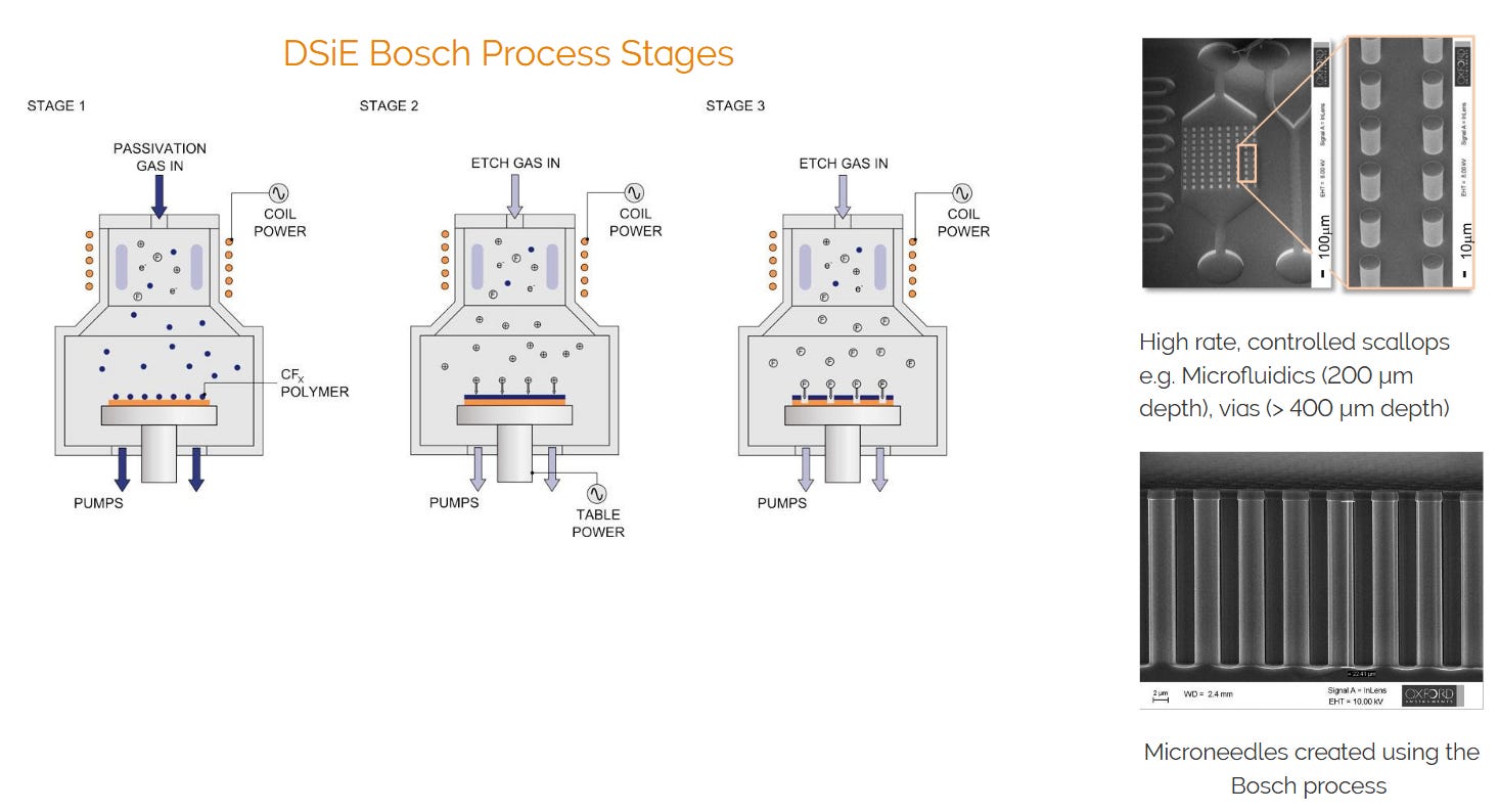
DRIE is a microfabrication technique used to etch deep and narrow features into silicon wafers with high precision. It is a key process in MEMS (Micro-Electro-Mechanical Systems) manufacturing and is particularly suited for creating microchannels, vias, and cavities with vertical sidewalls. The process alternates between etching and passivation steps to achieve high aspect ratios while maintaining structural integrity.
Copper Pillar Array for Enhanced Thermal Convection Paths
In addition to microchannels, TSMC has introduced the Copper Pillar Array as a supplementary structure to strengthen thermal convection pathways. These copper pillars can serve as micro-bumps or thermal columns, conducting heat directly from the active silicon layer and providing an additional solid-state thermal transfer path.
Copper, with its significantly higher thermal conductivity compared to TIM powders or phase-change interface materials, helps reduce local thermal resistance. When tightly integrated with the cooling fluid pathways, the copper pillar array significantly enhances system-level thermal dissipation efficiency.
TIM Material Research vs. No-TIM Architecture Innovation
TIM Material Challenges: Voids, Adhesion, and Reliability
Common issues with TIM1/TIM2 layers include:
Interface Voids: These reduce thermal connectivity and increase thermal resistance.
Poor Adhesion: Leads to delamination between layers.
Material Degradation: High temperatures can cause material failure and pump-out, where TIM is displaced over time.
Indium alloy TIMs (≈80 W/m·K) offer excellent thermal conductivity but require surface metallization (e.g., Ti/Au or Ni/Au) on the chip backside and lid, along with a reflow process to ensure low interfacial thermal resistance and high reliability.
No-TIM Architecture: A Breakthrough Innovation
TSMC has explored a Direct Water Cooling (DWC) architecture that eliminates the need for intermediate TIM layers. In this approach, microfluidic cooling channels are etched directly into the silicon die, enabling direct contact between the cooling fluid and the heat-generating active layer. This significantly reduces interfacial thermal resistance.
In comparative tests across three architectures:
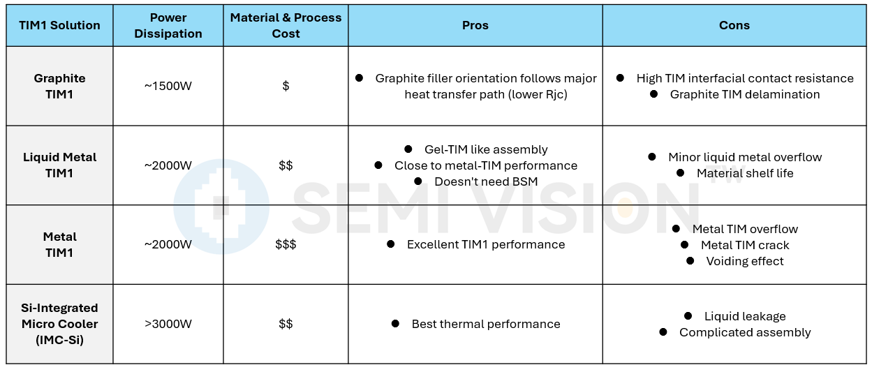
Pure DWC Architecture: Achieved 2.6 kW heat load with a ΔT of 63 °C — the best performance.
Oxide (OX) TIM Architecture: Reached 2.3 kW / 83 °C.
Liquid Metal TIM Architecture: Handled around 1.8 kW / 75 °C.
Among different microchannel structures, the pillar-based microchannel configuration demonstrated the most effective thermal performance.
For Paid Members,SemiVision will discuss topics on
System-Level Co-Optimization: Foundry-Led Direction for Future Thermal Packaging
The Thermal Wall Challenge of AI Chips: From Microchannel Liquid Cooling to TSMC's Chip-Level Thermal Management Technologies
AI Era Heat Flux Challenge: Hotspots Entering Overheating Zone
Key Limitations of Traditional Cooling
TSMC’s Perspective: Silicon Cooling Die and Chip-Level Thermal Solutions
Heat Meets Packaging: The New Era of Integrated Thermal Design
Key Advantages of Microchannel Cooling for Thermal Budget Enhancement
Recent Breakthroughs: Advanced Solutions to Push the Thermal Budget Further
Advancing Toward Microchannel-Based Chip Cooling: A Thermal Revolution for the AI Era
Microchannel Geometry and Packaging Challenges
Thermal Management Technologies and Their Corresponding Integration Levels
Microchannel Cooling: Targeted for Chip and Package Levels
The differences among the three microchannel section shapes for Microchannel Heat Sinks (MCHSs)
Visualization of Microchannel Flow Dynamics
Fabrication Processes for Microchannel Heat Sinks (MCHS) on Different Substrates
Future Applications: Conceptual Visualization of 3D IC and On-Chip Cooling Integration
Basics and Classification of TIM (Thermal Interface Material)
Impact on Chip Thermal Performance and Thermal Budget
TSMC’s Rationale for Advancing No-TIM Solutions
Key Challenges of Adopting Microchannel Cooling in SoW
Industry Frontline Developments and Future Possibilities
Thermal Challenges and Technology Trends in High-Power AI Chip Computing
Chip Thermal Budget and Thermal Resistance Management
Industry Strategies and Technological Developments
Future Challenges and Integrated Solutions for System-Level Thermal Management
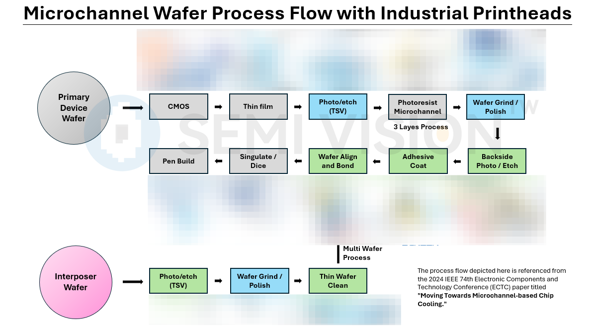
Microchannel Wafer Process Flow Explanation
Technical Significance and Application Expansion