


Munich Beams Ahead into Photonics 5.0: Where Laser Meets AI, Quantum, and Silicon
Original Articles By SemiVision Research (Laser World of Photonics, FiconTEC ,Femtum, PhotonDelta, EPIC, LioniX, Photonics21, OSRAM,TRUMPF, VLC, Foxconn,Wave Photonics,Suruga,EPIC,OPTICA)

Laser World of Photonics 2025 Highlights Pivotal Shifts in the Photonics Industry
The 2025 edition of Laser World of Photonics has officially opened in Munich, reaffirming its role as a global benchmark for photonics innovation. This year’s exhibition reflects a convergence of technologies—from traditional optical communication and precision metrology to silicon photonics, quantum optics, and nano/micro-scale fabrication—highlighting the industry’s transition toward system-level integration in response to the rising demands of AI, quantum technologies, and high-frequency applications.
Key themes emerging from the show include the rapid industrialization of silicon photonics testing and packaging solutions (such as double-sided testing and laser trimming), the expansion of THz communication and nonlinear wavelength conversion, the system-level maturity of quantum platforms (e.g., diamond NV centers and ion traps), and innovations in micro-3D structuring and glass-based packaging for high-reliability integration.
Driven by national initiatives, evolving system requirements, and intensified academic–industrial collaboration, Laser World of Photonics 2025 signals a clear inflection point: photonics is no longer just about device innovation—it is now redefining system architectures across industries. As the sector moves from R&D to manufacturing, and from fragmented components to cohesive platforms, photonics is becoming a structural backbone for the next era of computing and connectivity.
As the 2025 Laser World of Photonics opens in Munich, leading innovators in photonics from around the world have gathered to showcase breakthroughs spanning lasers, sensors, and optical interconnects. With the rise of AI and high-performance computing pushing bandwidth and energy efficiency to their limits, traditional electronic I/O architectures can no longer meet the growing demands of data centers. Against this backdrop, silicon photonics and optical interconnects are rapidly emerging as the backbone of next-generation data infrastructure.
This year’s exhibition highlights national pavilions and collaborative ecosystems from countries including the Netherlands, Canada, the United States, Israel, Switzerland, and Japan. These showcases demonstrate full-stack integration—from chip design, materials, and packaging to testing—while also underscoring the growing momentum of international cooperation in building a photonic-electronic convergence ecosystem. Key players such as PhotonDelta and PhotonicsNL at the Netherlands Pavilion, Canada’s INO-led national delegation, and German-based leaders like ficonTEC, ams OSRAM, and TRUMPF are setting the stage with integrated platforms and real-world applications that bring silicon photonics closer to commercial maturity.
Beyond core technologies, this event marks a paradigm shift for the LED industry itself. Once focused on lighting and displays, the sector is now entering the domain of optical interconnects—driven by collaborations with semiconductor leaders such as TSMC and Avicena, and targeting chip-to-chip (C2C) optical links. The future of high-speed computing and data movement is no longer just about going “faster and smaller,” but about redefining the system itself through the convergence of light and silicon.Laser World of Photonics 2025 Opens Grandly — FiconTEC’s Silicon Photonics Testing Solutions Take Center Stage

Today, the world’s most influential photonics event — Laser World of Photonics 2025 — officially kicked off in Munich. The exhibition brings together over a thousand top-tier companies and research institutions from around the globe, showcasing the latest developments across laser technologies, metrology systems, optical communications, silicon photonics, and advanced packaging.
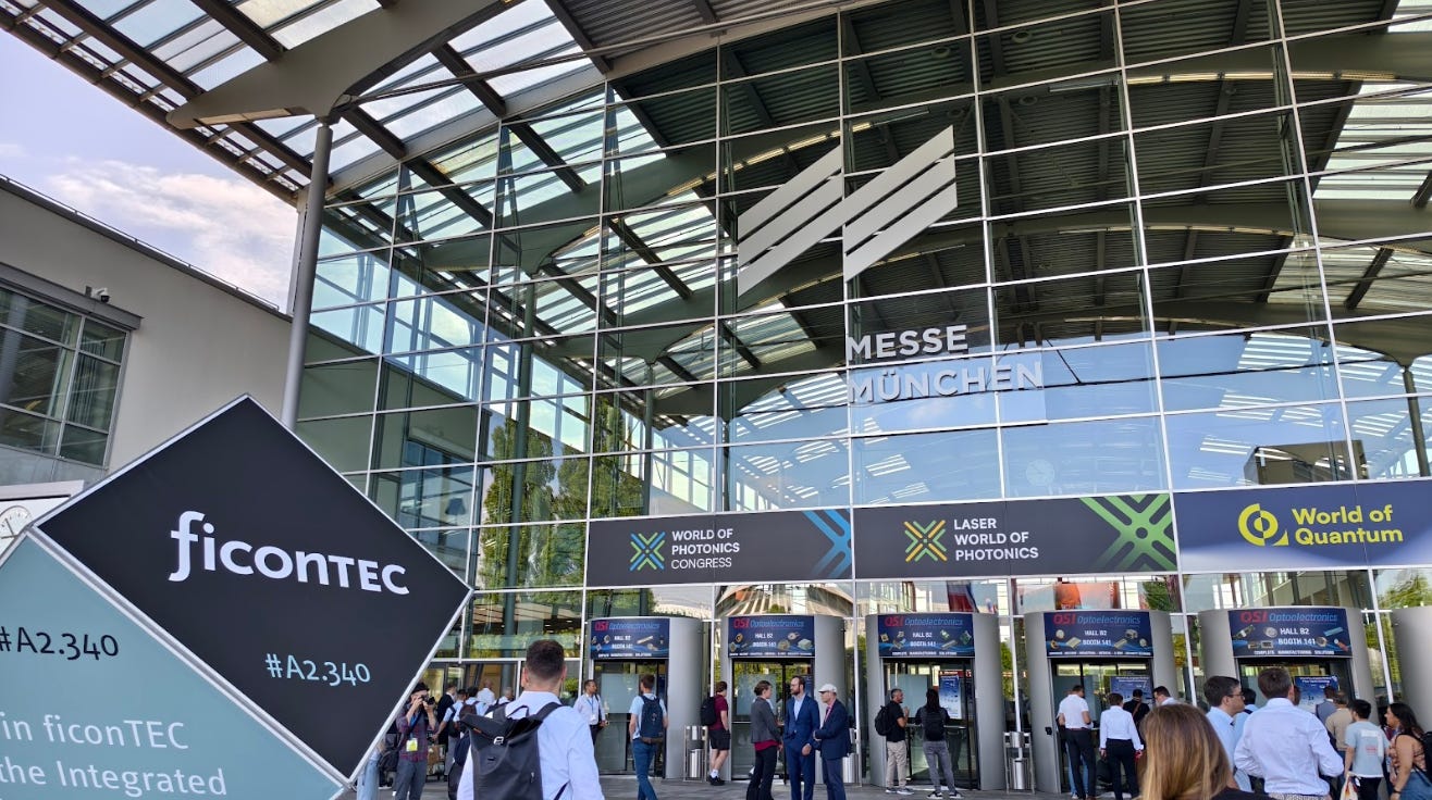
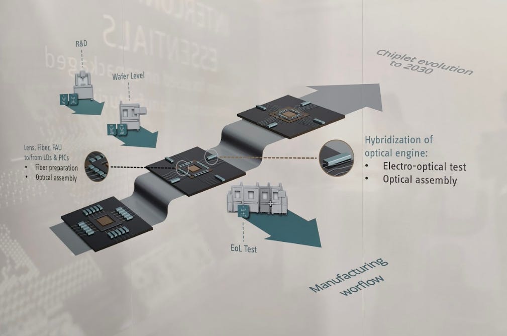
On opening day, FiconTEC captured attention with a prominent logo and its dedicated “Spotlight Zone” at the main entrance, signifying its leadership in optical assembly and testing. The company focused on one of the industry’s hottest topics: testing and rework solutions for Silicon Photonics (SiPh) and Co-Packaged Optics (CPO) systems.

As previously emphasized in our analyses: “Testing capabilities in silicon photonics are not just barriers to successful R&D — they are the key bottlenecks for mass production and yield optimization.” At this year’s event, FiconTEC unveiled a portfolio of innovations including wafer-level laser trimming, double-sided optical testing, and automated module alignment platforms — essential tools for engineers and strategists in SiPh manufacturing.
With 25 years of experience in optical alignment and high-precision testing, FiconTEC is accelerating the industry’s transition from “point testing” to system-level packaging validation, providing robust process support for next-generation high-speed optical interconnects required by AI and HPC chips.
Laser Wafer Trimming System: High-Throughput Optimization Tool for Silicon Photonics
Function and Purpose
The laser trimming technique injects permanent stressors into the wafer to adjust interferometer arm lengths, achieving spectral calibration, energy savings, and reducing reliance on thermal tuning. This method not only calibrates Good Dies but can also salvage Bad Dies, transforming them into usable components.
Industry Application
FiconTEC, in partnership with Femtum (Canada), introduced the first Photonics Wafer Laser Trimming System featuring microsecond-level waveguide tuning and a dry laser cleaning module. The system boosts Known-Good-Die (KGD) yield and ensures surface integrity.
Double-Sided Wafer Testing: Embracing the 3D Stacking Era
Current Development
Although not yet exhibited, FiconTEC’s upcoming tool supports 300 mm wafers and more rigid formats such as “COUPE wafers”, designed for 3D stacked optical engine chips (e.g., NVIDIA’s architecture). The platform enables top-and-bottom-side optical and electrical interface alignment, compensating for up to 2 mm wafer warpage using vacuum chucking and surface profile correction.
Ecosystem Integration
Deep collaboration with Teradyne, Advantest, and Keysight allows seamless compatibility with ATE platforms (e.g., UltraFLEXplus), enabling high-throughput SiPh and CPO testing environments.
FiconTEC’s Core Advantages
1. 25 Years of Optical Alignment Expertise
Unlike competitors from traditional semiconductor test backgrounds, FiconTEC originated from precision optical alignment, offering sub-micron beam tuning capabilities.
2. Modular System Architecture
Supports swappable modules such as FAU (Fiber Array Unit), laser trimming heads, and dry cleaning units; designed for integration into existing ATE systems.
3. Complete Test Coverage
From single-sided to double-sided, die-level to module-level testing, the platforms support RF testing from 70 GHz to 110 GHz with only probe card or instrument adjustments.
Solving Industry Bottlenecks
Warped Wafer Handling:
Thin wafers often exhibit curvature. FiconTEC applies vacuum chucks and adaptive surface compensation to stably process wafers with up to 2 mm warpage.
2.8 µm Laser Cleaning Technology:
This wavelength is transparent to silicon substrates but effective at ablating water and contaminants — enabling non-chemical, high-efficiency, and AR-coating-safe cleaning.
Innovative Optical Alignment:
Supports both grating and edge coupling configurations; FAU tips can utilize 3D-printed lenses to enable vertical coupling for more flexible test setups.


Future Trends and Market Opportunities
The industry is evolving from discrete modules → co-packaging → full chip-level integration. Leaders like NVIDIA are pushing toward optical testing standards, as Optical I/O becomes a central element in future high-speed interconnects.
FiconTEC’s diversified systems — covering single/double-sided ATE-compatible testing, laser trimming, and FAU-based optical probing — are becoming key nodes in the SiPh supply chain, offering comprehensive, future-proof solutions for the AI era.

Why Advanced Package Testing Matters
Advanced packaging — especially 2.5D/3D integration using interposers and Through-Silicon Vias (TSVs) — drastically increases packaging complexity. You now have multiple dies, interposers, and substrates in one stack, making reliability and yield heavily dependent on verifying connectivity between both sides of the wafer or interposer .
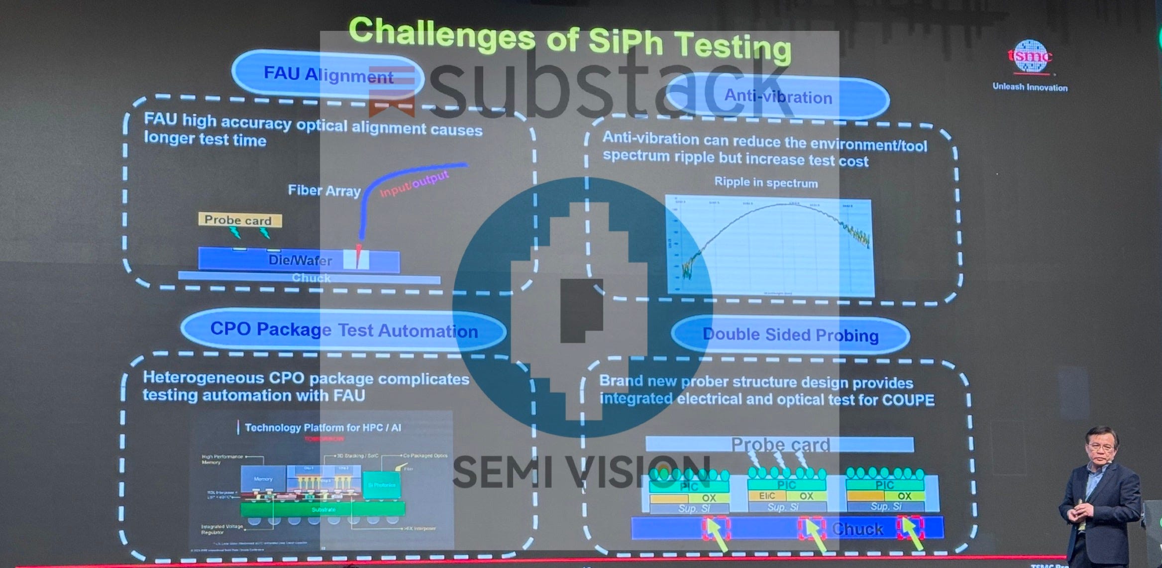
Double-Side Testing in Silicon Photonics
When applied to silicon photonics platforms, double-side testing is not merely an extension of standard process verification—it is a critical step in ensuring the reliability of electro-photonic integration. As silicon photonic modules evolve from single optical devices to complex heterogeneous integrations (e.g., PIC + EIC, or PIC + interposer + ASIC), the difficulty of testing increases significantly—especially when both electrical and optical signal paths must be validated simultaneously.
In this context, double-side testing refers to probing both the top surface (containing photonic devices and metal routing) and the bottom surface (e.g., for laser bonding, TSVs, or fiber coupling interfaces) to verify functionality. Key objectives include:
Alignment accuracy verification of photonic structures: Ensuring that microring modulators, photodetectors, and coupling structures are not misaligned during packaging.
Integrity check of both electrical and optical paths: Validating power/signal lines and optical connections such as FAUs or grating couplers for proper performance and minimal insertion loss.
Known-Good PIC verification prior to assembly: Utilizing dual-side probe cards and optical alignment systems to screen PICs before entering the packaging stage, thus improving initial yield.
Integration with wafer-level laser trimming and dual-side optical testing: For tunable resonators or coupling structures, advanced packaging flows often combine dual-side laser adjustment with optical probing to optimize spectral response and power efficiency.
Double-side testing thus plays a pivotal role in silicon photonics manufacturing. It improves die stacking yield, ensures consistent module performance, and lays the groundwork for scalable and standardized testing of large-scale silicon photonics systems such as CPO (Co-Packaged Optics), OIO (Optical I/O), and quantum sensing modules. For players like TSMC and ASE, it is an indispensable engineering step in building integrated photonic packaging platforms.
ASE’s Position
As the largest OSAT globally, ASE is investing heavily in advanced packaging and testing capabilities. In 2025, ASE projects 75% of its $1.6 b revenue from advanced packaging processes, including extensive double‑side testing for AI chips and interposer stacks .
Key rationale: Testing early-tier modules ensures high yield and prevents downstream failures.
ASE’s subsidiary, Siliconware Precision Industries, has been collaborating with Nvidia for decades, jointly validating advanced packaging steps — presumably including double‑side test protocols .

TSMC’s Approach
TSMC has integrated double‑side and wafer-level probing into its advanced 3DFabric™ ecosystem (CoWoS®, InFO, SoIC):
Ensures interposer die are known‑good before assembling
Enables validation of functional stacking in intermediate steps
TSMC’s formation of a 3DFabric Alliance with OSATs and test partners underscores how critical early and multi-tier testing is to complex heterogeneous integration .
Nvidia’s Reliance
Nvidia, a leading driver of 2.5D packaging for AI GPUs, demands exceptional interconnect performance to achieve bandwidth >4 TB/s:
Their HBM-GPU stacks require precise signal integrity, which is ensured only through rigorous testing across both sides of the stacked structure.
Failures in early bonding/interposer layers compromise the entire module — making double‑side testing essential .
Supporting data bandwidth and thermal constraints in multi-chip integration, Nvidia works closely with ASE and TSMC on double‑side and known‑good-die (KGD) verification workflows.


Spotlight on Quantum Computing Integration Challenges
The event also touched on Quantum Computing, a field full of promise but significant challenges. One standout was NEXT, a company with deep expertise in the field.

In quantum architectures, integrating optical and electronic control presents a major hurdle. For trapped-ion systems, physical size remains a limiting factor — due to large lasers and acousto-optic modulators (AOMs), these systems can’t easily scale down to micron-level like semiconductors. However, embedding these control elements onto chips — even within vacuum environments — remains critical to advancing compact, scalable quantum processors.

Global Quantum Computing Landscape and Strategic Directions
United States
The U.S. leads in quantum computing through the National Quantum Initiative Act, coordinating efforts among tech giants such as Google, IBM, and Intel, as well as national labs and academic institutions. The primary focuses are superconducting qubits, topological qubits, and quantum networking. IBM, in particular, plans to launch a 4,000+ qubit processor by 2025, aiming to strengthen commercial deployment and cloud-accessible quantum platforms.
Europe
Europe is advancing under the decade-long Quantum Flagship initiative, with multinational collaboration at its core. The program covers quantum communication, sensing, and simulation. Countries like Germany and the Netherlandsemphasize localizing the quantum supply chain, with key players including QuTech in the Netherlands and Europe’s quantum chip development platforms like IMEC playing pivotal roles.
China
China adopts a centralized national investment strategy. Major achievements include the world’s first quantum satellite “Micius” and the Beijing-Shanghai quantum communication backbone. The country is making strong progress in both optical quantum computing and trapped ion systems, moving toward the development of large-scale, feasible quantum architectures.
Japan and South Korea
Japan and South Korea pursue dual-track approaches with superconducting and photonic technologies. Japan’s NTT, University of Tokyo, RIKEN, and NEC are particularly active in superconducting qubits and silicon-based quantum dot platforms through academia-industry collaboration.
NVIDIA’s Strategy on Quantum Computing
NVIDIA takes a “quantum simulation + AI-assisted development” approach, emphasizing the synergy between classical and quantum computing. Its cuQuantum SDK enables large-scale quantum circuit simulations on GPUs, accelerating algorithm verification and quantum error correction research. NVIDIA is partnering with emerging quantum players like Google and IonQ.
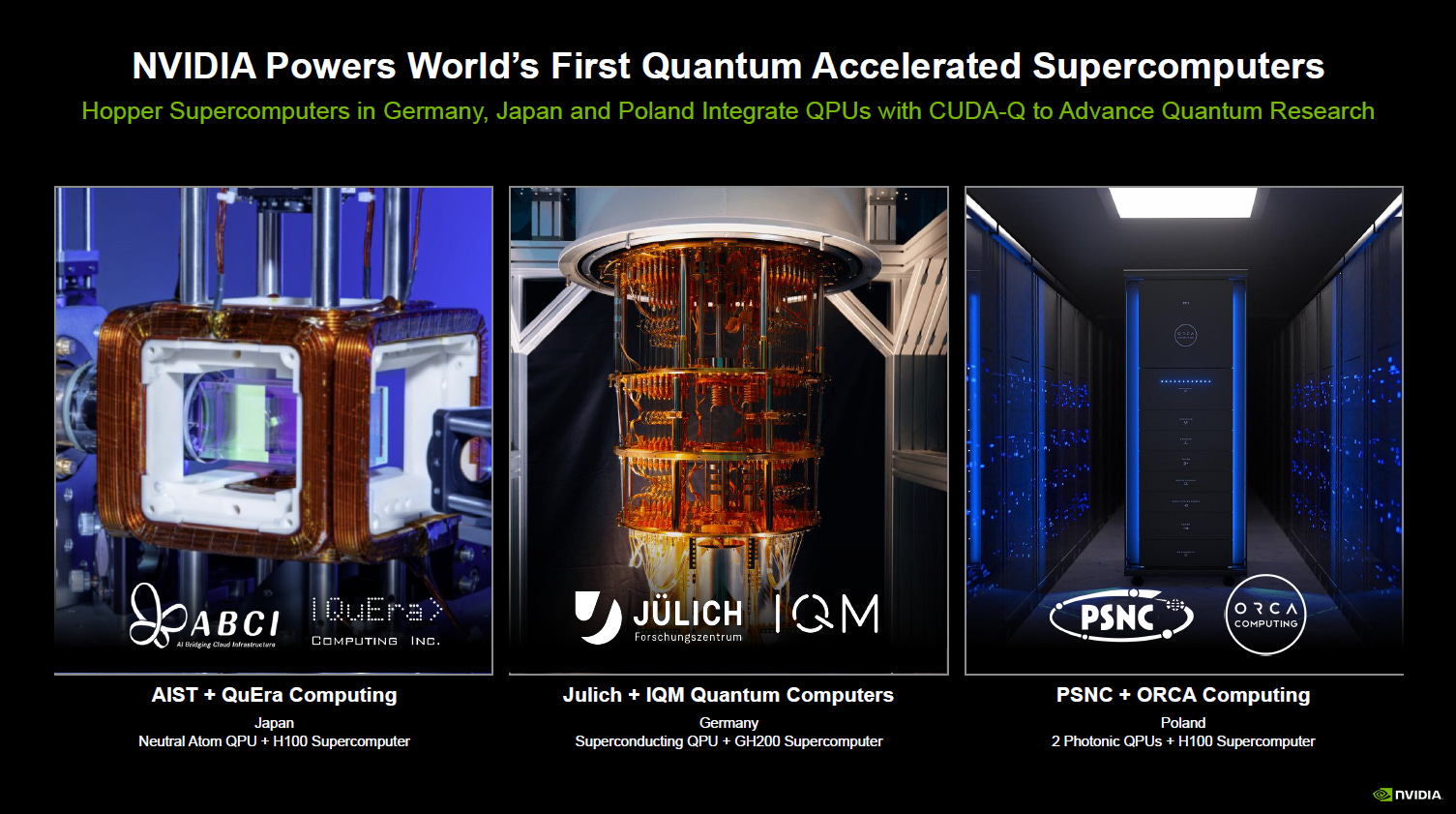
Rather than developing its own quantum hardware, NVIDIA focuses on building a “quantum acceleration platform,”positioning its GPUs as a backbone for quantum simulation and early-stage research. The company believes that in the near term, quantum computers must be deeply integrated with classical supercomputers to maximize computational efficiency.
Quantum Development in Taiwan
While Taiwan lacks large-scale quantum hardware players like Google or IBM, it has launched a coordinated academic and talent development effort. In 2022, Taiwan’s Ministry of Science and Technology initiated the Quantum Technology Flagship Program, bringing together institutions like National Tsing Hua University, National Taiwan University, and Academia Sinica to advance research in quantum computing, communication, and materials.
Taiwan’s hardware research focuses on superconducting qubits and silicon-based quantum dots, with some teams also exploring photonic chips and single-photon detectors. Chip design and front-end fabrication are still reliant on international foundries such as TSMC, which could become a key enabler in aligning with global silicon photonics processes.
Quantum Strategies from Foxconn Research Institute and Academia Sinica

The Foxconn Research Institute has established an international collaboration framework for quantum information science, emphasizing industrial applications. Leveraging its strengths in packaging, power modules, and optoelectronics, Foxconn is advancing development in quantum sensing and communication components. Its quantum team collaborates with academic institutions in the U.S. and Europe, aiming to build a mass-producible quantum component platform.

Academia Sinica, on the other hand, focuses more on fundamental theory and experimental validation, including work on quantum entanglement, many-body quantum theory, superconducting qubit control, and quantum simulations. It collaborates with top universities such as NTHU and NYCU on chip design and optoelectronic device testing. The institute also actively participates in Asia-Pacific quantum network initiatives (e.g., APQN), helping integrate Taiwan into the global quantum research ecosystem.

The future of quantum computing is not solely a hardware race — it is a comprehensive, global integration of research, talent, and industrial application. If Taiwan can leverage its strengths in IC design, optoelectronic manufacturing, and advanced packaging/testing, it stands a strong chance of capturing value in the application layer of this long-term quantum technology competition.
Optical Computing and Room-Temperature Quantum Traps
Challenges in Trapped-Ion Quantum Integration and the Need for Cross-Industry Collaboration
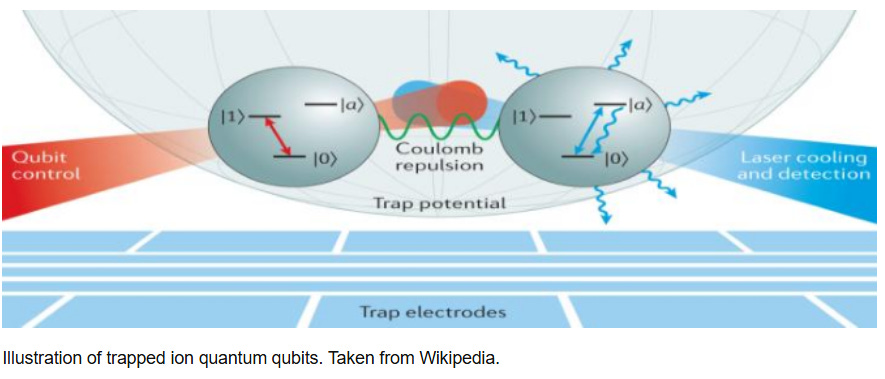
As quantum computing advances toward practical deployment, trapped-ion systems have emerged as one of the most promising architectures. These systems combine highly stable qubits, precise quantum logic gates, and the potential for room-temperature operation. However, their development faces significant physical and engineering challenges in optics, electronic control, and system integration. This article examines these hurdles from three perspectives: integration bottlenecks, the contrast with traditional computing, and the industrial collaboration required to realize scalable solutions.
1. Optical Component Integration Constraints: Bottlenecks from Lasers to AOMs
1.1. Size Barriers of Lasers and AOMs
Precise manipulation of internal ion states relies heavily on laser control. Trapped-ion systems currently depend on free-space lasers and Acousto-Optic Modulators (AOMs) for fine control. These components are bulky and require fixed optical paths. AOMs are physical crystals that operate via free-space beam passage and cannot be integrated as system-on-chip (SoC) elements, limiting system miniaturization.
1.2. Fixed-Wavelength Constraints
Trapped-ion systems typically operate at 532 nm, differing from the 850–1550 nm wavelength range standard in CMOS technologies. This discrepancy prevents compatibility with existing nanofabrication scaling technologies and limits the potential to miniaturize both optical and control components.
1.3. Physical Size of the Trap
A typical ion trap measures about 20 mm × 20 mm, with the smallest structural features around 20 µm. These complex 3D structures limit the achievable qubit density per unit area, even if the control circuits are partially miniaturized.
2. Fundamental Differences from Traditional Computers

The design and scaling of trapped-ion systems do not follow Moore’s Law. Unlike conventional computers, they cannot rely on advanced packaging or wafer-level integration to increase qubit density and computational efficiency.
3. Cross-Disciplinary Collaboration: A Prerequisite for Scalable Trapped-Ion Quantum Systems
3.1. Semiconductor Industry: Enabling On-Chip Electronic Control
TSMC: Can assist in developing CMOS control circuits operable in vacuum environments.
Infineon: Brings expertise in high-voltage and radiation-hardened devices, crucial for trap control and laser drivers.
3.2. Photonics Industry: Miniaturizing Lasers and AOM Modules
Laser modules need further size reduction and integration, possibly leveraging silicon photonics for partial modulation functions.
AOMs require planar waveguide alternatives or the use of new materials for achieving on-chip acousto-optic effects.
3.3. RF System Vendors: Supplying High-Voltage, Precision RF Sources
Development of low-noise, vacuum-compatible RF drivers capable of outputting 1000V @ 50 MHz is essential.
3.4. Thermal Management and Vacuum Chamber Design
Ion cooling relies on stable laser-based cooling systems, which must incorporate multi-mode lasers and fast thermal control loops.
Vacuum chambers must be co-designed with control modules, demanding high standards in materials and mechanical engineering.
3.5. System Integration and Commercialization
While Taiwan and parts of Europe have strengths in subsystem manufacturing, experience in turning prototypes into reliable products remains limited.
A complete ODM / volume production and test validation ecosystem must be built.
From “Impossible” to “Manufacturable”
Trapped-ion quantum computers now stand at the crossroads of experimentation and commercialization. The primary challenge is no longer the qubits themselves, but the integration of large-scale optical components, vacuum systems, and electronic controls into manufacturable, testable, and scalable platforms.
Success depends on multi-industry collaboration — from semiconductors to photonics, lasers, materials, RF systems, and packaging.
Whether it’s TSMC, Infineon, laser module vendors, or silicon photonics packaging houses, each technological domain holds a piece of the puzzle. Their collaboration will form the foundation for the era of practical quantum computers.
Nanoscribe GmbH & Co. KG: Global Leader in Micro/Nano-Scale Two-Photon 3D Printing

Nanoscribe GmbH & Co. KG is the world’s first company to successfully commercialize Two-Photon Polymerization (2PP) technology. Founded in 2007 as a spin-off from the Karlsruhe Institute of Technology (KIT)in Germany, Nanoscribe is now part of the high-tech industrial group Lab14, with locations in Germany, the United States, and China, serving customers across Europe, North America, and Asia.

Nanoscribe specializes in high-precision 3D printing at the micro- and submicron scale, offering innovative microfabrication platforms for advanced applications in optics, photonics, biomedical engineering, MEMS, and semiconductor packaging. Its flagship commercial platform, the Quantum X series, supports a wide range of modular systems and application modes, including align printing, bio printing, and little mastering for micro-mold fabrication.
Core Technologies and Key Applications
At the heart of Nanoscribe’s platform is two-photon polymerization 3D printing, a technique that focuses ultrafast lasers into photosensitive polymer resins to induce nanoscale point-by-point curing. This allows for the creation of extremely fine three-dimensional microstructures. The printing resolution reaches down to 100–200 nanometers, supporting the fabrication of freeform micro-optical components such as aspheric lenses, freeform couplers, and 3D topographic patterns.
One of its standout systems, Quantum X align, features automated alignment printing, enabling recognition of fiber cores, chip edges, and fiducial marks. This allows for direct printing of micro-optical components or beam-shaping structures on specific surfaces, making it highly applicable to silicon photonics (SiPh) chip packaging, quantum chip optical coupling, fiber array alignment, and high-density integration scenarios.
In addition, Nanoscribe offers a bio-specific printing platform compatible with hydrogels and biodegradable materials for applications in cell culture, microfluidics, and regenerative medicine scaffolds.
Commercial Applications and Industry Expansion
Nanoscribe was the first company to bring two-photon polymerization out of the lab and into commercial industries. It now serves over 4,000 academic and industrial users, including top institutions such as MIT, Harvard, ETH Zurich, and IBM Research. Its commercial applications span:
Micro-optics: Freeform microlenses, waveguide couplers, diffractive optical elements (DOE), fiber end-face optics
Semiconductor Packaging: SiPh optical alignment, laser coupling interfaces, master mold replication, and test structures
Biomedicine and Microfluidics: Micro scaffolds, cell adhesion platforms, 3D microchannel systems
Vertical Structures and Surface Roughness Control: For precision processes that require strict SR and step height control
3D Mapping Applications: Printing of arbitrary shapes and topologies, integration with metal modules and microstructure metrology
Future Development Directions
Looking ahead, Nanoscribe aims to strengthen its global leadership in two-photon fabrication by advancing along several key strategic paths:
New Materials and Multi-Functional Printing: Development of high-transparency and biocompatible materials such as IPX-Clear and bioresins
Industrial Automation and Volume Production: Supporting large-area printing, automated handling, and high-throughput packaging processes
Deep Expansion into Asian Markets: Accelerating adoption through partnerships with leading optoelectronic and semiconductor companies in Taiwan, South Korea, and Japan
Cross-Industry Platform Expansion: Extending beyond optics and semiconductors into areas such as advanced sensing and biomedical MEMS
Global Technology Branding: Enhancing its image as a global technology leader in Asia and North Americathrough strategic media and expert content dissemination
Nanoscribe’s business model is evolving from that of a high-end research tool supplier to a cross-industry microfabrication solutions partner. With its precise printing technologies, diverse materials platforms, and deep understanding of packaging needs, Nanoscribe is well-positioned to become a key enabler in emerging areas such as photonic packaging, quantum chip manufacturing, and 3D optical coupling.
NTT Innovative Devices: Technology Highlights at Laser World of Photonics
At this year’s Laser World of Photonics, NTT Innovative Devices showcased a broad array of advanced modules and components spanning optoelectronics, terahertz (THz) communication, nonlinear wavelength conversion, biomedical microfabrication, and visible-light PIC platforms, reinforcing its position as a forward-looking innovator in the photonics industry.
Terahertz Communication Modules: High-Speed Interfaces with 3D-Printed Waveguide Integration
NTT presented a comprehensive THz interface module system covering a bandwidth range of 220–300 GHz. The system integrates optical modulation, photodetection, frequency mixing, and broadband power amplification. Using UTC photomixers, FMB diode modules, and WR3.4 waveguide structures—including 3D-printed waveguides—the platform supports high-speed data signal processing, multiplexing/demultiplexing (MUX/DEMUX), and efficient frequency mixing and amplification, making it ideal for ultra-high-speed wireless communication and advanced measurement applications.
DFB Lasers for Gas Sensing: Bridging Communication and Spectroscopy
NTT also exhibited several Distributed Feedback (DFB) semiconductor laser modules, covering the 1260–2340 nmwavelength range, optimized for gas absorption spectroscopy. These lasers enable precise sensing of gases such as CO, CH₄, NH₃, NO, and H₂O, and feature TEC thermal control and 14-pin packaging.
NTT’s latest laser lineup includes:
2 μm DBR lasers
RTF tunable lasers
Integrated coaxial modules
These are applied in breath analysis, temperature sensing, LiDAR, OCT, and drone sensors, expanding the company’s presence in emerging sensing markets.
PPLN Wavelength Conversion Modules: Tunable Nonlinear Light Sources
To meet the growing demand for multi-wavelength optical sources, NTT introduced PPLN (Periodically Poled Lithium Niobate) waveguide modules, supporting Second Harmonic Generation (SHG), Sum Frequency Generation (SFG), and Difference Frequency Generation (DFG).
The modules integrate:
Thermoelectric cooling
Thermal sensors
Ridge waveguide designs
These features enable high conversion efficiency and stable light output, outperforming traditional bulk PPLN by 1–2 orders of magnitude. Target applications include quantum optics, infrared sensing, and medical light sources.
Microfluidic Glass Chip Fabrication: High-Precision MEMS Integration Platform
NTT demonstrated capabilities in microchannel processing on silicon and glass substrates, enabling multi-layer channel structures exceeding 40 μm. Combined with PDMS imprinting techniques, these chips achieve high stability and throughput, ideal for fluorescent particle sorting and flow simulation applications. Potential extensions include biochips, lab-on-chip systems, and sensitive chemical reaction platforms.
Visible-Light PIC Modules: High-Power, Integrated Photonics Platform
The visible-light PIC module presented by NTT features:
445 nm laser output at 100 mW
RGB multiplexed coupling (Red: 650 nm, Green: 520 nm, Blue: 450 nm)
Insertion loss < 1 dB
Built on mature telecom-grade photonic integrated circuit (PIC) technology, the module is compact and highly reliable. It is well-suited for:
Augmented reality (AR) glasses
Scanning ophthalmoscopes
Flow cytometers
Fluorescence microscopy
And other wearable and precision medical devices
Positioning in the Future of Photonic Systems
NTT Innovative Devices’ exhibition covered a complete spectrum—from far-infrared to visible light, and from silicon photonics to THz frequencies. This demonstrates not only technological breadth but also a deep understanding of component miniaturization, integration, and commercialization trends.
With diversified packaging platforms, nonlinear light source modules, visible-light PICs, and high-precision microfabrication capabilities, NTT is positioning itself as a core enabler in next-generation communications, biomedical sensing, and optical measurement systems. These technologies form a foundational component base for silicon photonics, quantum optics, and future optical interconnect architectures.
XeedQ: Building Mobile and Scalable Quantum Processing Platforms

XeedQ is an innovative company focused on developing portable quantum processors and related infrastructure, emphasizing modular, scalable, and high-reliability quantum computing platforms. Its flagship product, the XQ1 series mobile quantum processor, is built around diamond NV center technology and integrates stabilized electronic and optical modules to provide users with deployable and easily integrable quantum computing capabilities.
Core Technology and Hardware Architecture
XeedQ’s quantum processor platform consists of several key modules:
Temperature-Controlled Electronic Stabilization Module: Ensures thermal stability during qubit operation.
Stabilized Optics Box: Handles laser signal generation and optical read/write operations.
Diamond Chip: The core quantum component that leverages NV (nitrogen-vacancy) centers for quantum state manipulation and readout.
Microscope Module and Control System: Supports high-resolution observation and quantum state initialization.
Pulse Synthesizer and Classical CPU Controller: Performs waveform generation, logic control, and hybrid computational tasks.

All modules are integrated into a portable rack unit, complete with a built-in display and keyboard, making the platform suitable for data centers, labs, and field deployment for quantum processing and measurement tasks.
Application Domains of the XQ1 Platform
XeedQ’s XQ1 series processors are designed for a broad range of use cases:
6G Communications and Network Optimization: Enables low-latency, high-security quantum-enhanced routing and signal processing.
Education and Training: Ideal for universities and quantum training programs for hands-on learning and algorithm simulation.
Material Simulation and Battery Research: Facilitates quantum simulations of new materials and molecular structures, with applications in semiconductors and green hydrogen industries.
HPC Integration: Can be paired with existing supercomputing systems to enhance AI model training, optimization, and scientific computing.
Quantum Random Number Generation: Supports true randomness for financial, defense, and cybersecurity applications, ensuring secure encryption and communications.
Ecosystem and Research Partnerships
XeedQ collaborates with several top European research institutions and universities, including:
German Aerospace Center (DLR)
Technische Universität Dresden
Goethe University Frankfurt
Fraunhofer, EPFL, HZDR, IONOPTIKA, Wiesner, SCHOTT, and other technology institutes and materials companies.
These partnerships reflect XeedQ’s strategic focus on applying its technologies across academic, industrial, and defense sectors.
Market Positioning and Vision
What sets XeedQ apart is its focus on practical deployment and integrability of quantum computing. Rather than focusing solely on lab-scale performance, the company emphasizes mobility and industrial integration, aiming to create quantum platforms akin to GPUs or edge computing modules—designed to become central processors in smart factories, communication base stations, and secure systems of the future.
With strong support from German government agencies such as the Federal Ministry for Economic Affairs and Climate Action and the Ministry of Education and Research, XeedQ is rapidly advancing toward commercialization. The company’s long-term goals include realizing Quantum-as-a-Service (QaaS) and establishing quantum edge platforms as deployable and accessible quantum resources for a wide range of real-world applications.
Bluefors: A Global Leader in Quantum Cooling Technologies
Bluefors is one of the most trusted ultra-low-temperature system providers in the global quantum computing and cryogenic application space. The company is dedicated to delivering stable, efficient, and scalable cooling platformsthat enable quantum systems — from single qubits to systems with up to 1,000 qubits — to operate reliably at cryogenic temperatures.
At the core of Bluefors’ technology is the dilution refrigerator, which creates an extremely low-temperature environment necessary for maintaining quantum coherence. Known for their modular design, precision engineering, and exceptional build quality, Bluefors systems are widely adopted across leading quantum labs and commercial quantum processor developers worldwide.
At this year’s exhibition, Bluefors unveiled a cooling hierarchy model with gold-plated thermal shielding, elegantly showcasing the architecture of a quantum computer’s thermal infrastructure — including the cold head, radiation shields, mechanical support structures, and electrical signal interfaces. This tangible model helped attendees understand both the design logic and engineering challenges of cryogenic quantum systems.
The company’s motto, “Cool for Progress,” reflects not only its confidence in its technological capability but also its strong commitment to supporting the advancement of the quantum industry. As the world moves toward the era of 100–1,000-qubit systems, Bluefors is building the thermal foundation essential for the next generation of quantum computing.

TECNISCO Ltd.: Precision Microfabrication for Advanced Packaging
Headquartered in Tokyo, TECNISCO Ltd., a subsidiary of The GOOD SYSTEM CORP., is a leading specialist in precision microfabrication and advanced material integration, particularly in the field of advanced packaging for semiconductor and optoelectronic applications.
Key Technologies and Product Capabilities
1. Through-Glass Via (TGV) and Glass Packaging Solutions
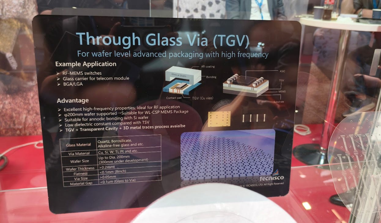
TECNISCO offers a full suite of TGV processing solutions, including thin-film deposition, via filling, bonding, and etching — supporting high-density, low thermal expansion, and high-frequency transmission requirements. Materials include fused silica and borosilicate glass, with excellent dimensional accuracy and surface flatness.
2. Glass Bonding Technologies
The company provides multiple bonding methods such as fusion, laser, and adhesive bonding, enabling custom cavity glass solutions with bottom or sidewall transparency — widely used in photonic components, sensors, and protective enclosures.
3. Metal-Diamond Composites
Products such as T1K, arcDia, and SbsDia offer high thermal conductivity and low thermal expansion, ideal for high-power devices, radar systems, power modules, data center cooling, and space electronics. These materials deliver excellent thermal management and packaging compatibility.
4. Electroplating and Surface Finishing
TECNISCO provides precision metal plating (copper, nickel, gold, silver, etc.) with surface roughness as low as Ra < 0.05 μm, suitable for high-reliability packaging. Layer thickness and structure can be tailored to customer specifications.
5. Dimensional and Custom Capabilities
Supports material thicknesses from 0.1 mm to 5 mm and processing widths up to 200 mm, utilizing laser, CNC, and grinding techniques for varying levels of precision and complexity.
Application Domains
Aerospace and Radar Systems (Space, Defense)
High-Frequency Power Modules
Data Center Thermal Management
High-Performance Packaging for CPUs/GPUs, MMICs, and ASICs
TECNISCO combines advanced microfabrication expertise with innovative material processing to enable the development of high-density, high-performance, and high-reliability electronic and photonic systems. It is recognized as a key supplier in the fields of advanced semiconductor packaging and optical component material solutions.
VLC Photonics: A Hitachi Group Company Driving Full-Stack PIC Integration
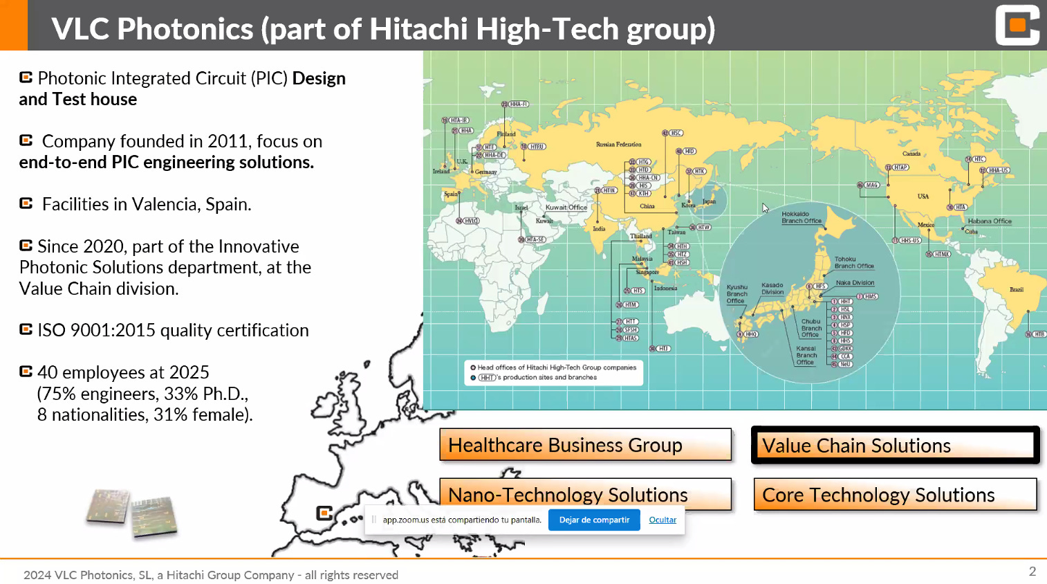
VLC Photonics, a company under the Hitachi Group, specializes in the integration and end-to-end services of Photonic Integrated Circuits (PICs). Offering a comprehensive pipeline from prototyping to volume production, VLC supports all six key stages: design, manufacturing, testing, packaging, system assembly, and validation. Its applications span optical communications, sensing, optical accelerators, AI inference, and AR/VR systems.
With multi-platform design and testing capabilities, VLC handles technologies based on III-V materials (e.g., InP, GaAs) and silicon photonics platforms (e.g., SOI, SiN). Its proprietary component libraries support passive devices (MMIs, splitters, ring resonators) and active devices (lasers, modulators, photodetectors), catering to a wide range of customer needs.
VLC collaborates with multiple foundries to support diverse material platforms and processes, providing services from small-batch prototyping to full-scale production. The company also offers customized PDK support, parameter modeling, and layout implementation, optimizing cost and performance according to client requirements.
For testing and packaging, VLC provides solutions including standard packaging substrates, ceramic interposers, fiber coupling designs, TEC thermal control, and partners with third-party OSATs for mass production scaling. Overall, VLC Photonics is a reliable PIC development partner with deep technical integration, platform diversity, and manufacturing flexibility—ideal for organizations accelerating the path from R&D to commercialization.
Suruga Seiki Co., Ltd.
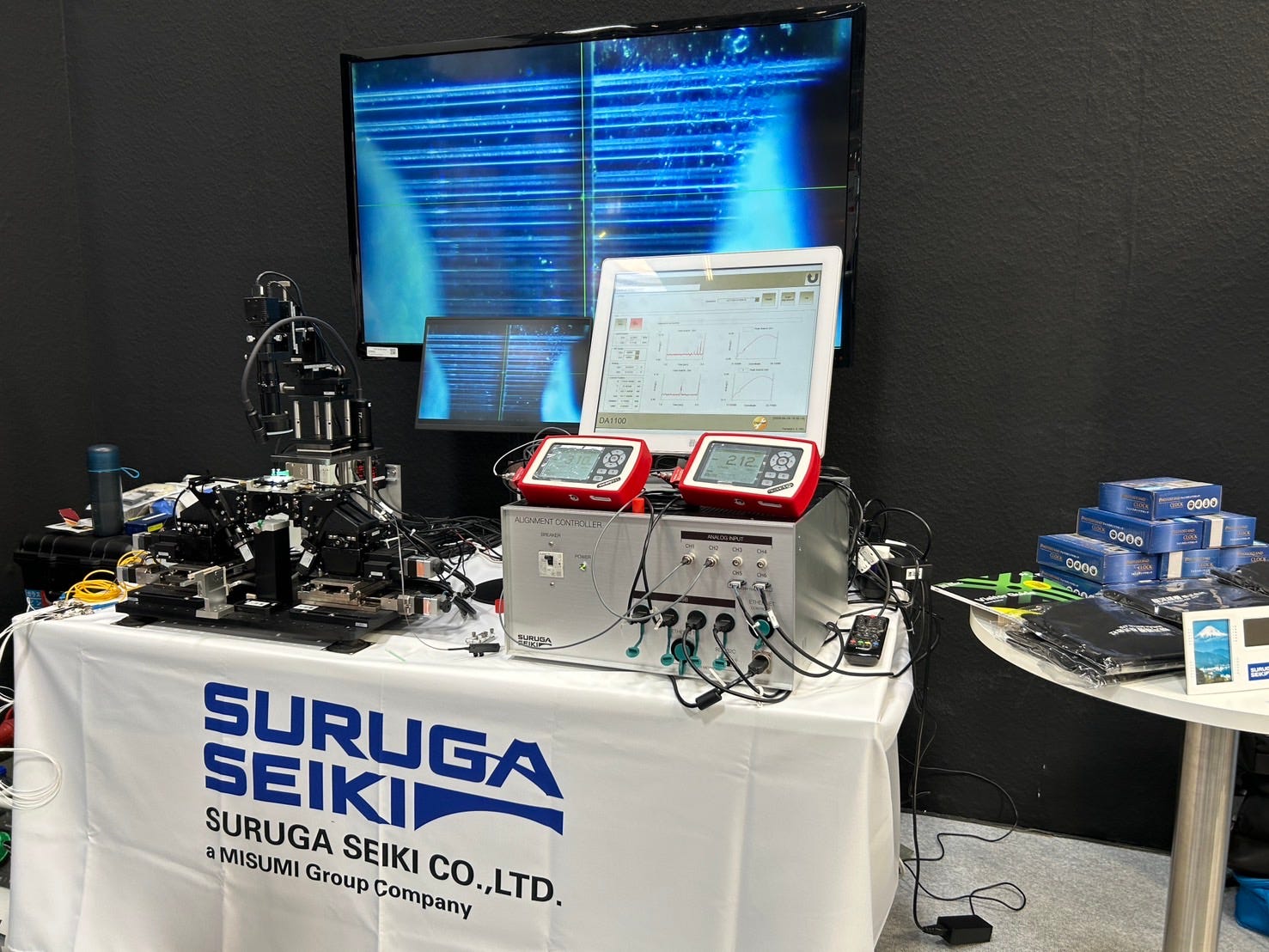
Suruga Seiki is a global leader in ultra-precision positioning and photonics automation solutions, headquartered in Japan. With decades of expertise in mechanical and optical alignment systems, Suruga specializes in high-precision motion stages, active/passive alignment modules, and optoelectronic packaging tools that meet the demanding requirements of silicon photonics (SiPh) and co-packaged optics (CPO).
At Laser World of Photonics 2025, Suruga demonstrated its advanced alignment platform featuring real-time monitoring and high-resolution control systems—empowering applications such as fiber-to-chip coupling, wafer-level photonic device testing, and PIC assembly automation.
By integrating precision engineering with AI-assisted controllers, Suruga Seiki continues to support next-gen optical communication and semiconductor packaging, providing scalable and reliable solutions for the photonics ecosystem.
Wave Photonics: Design-Driven Innovation for Scalable Photonics
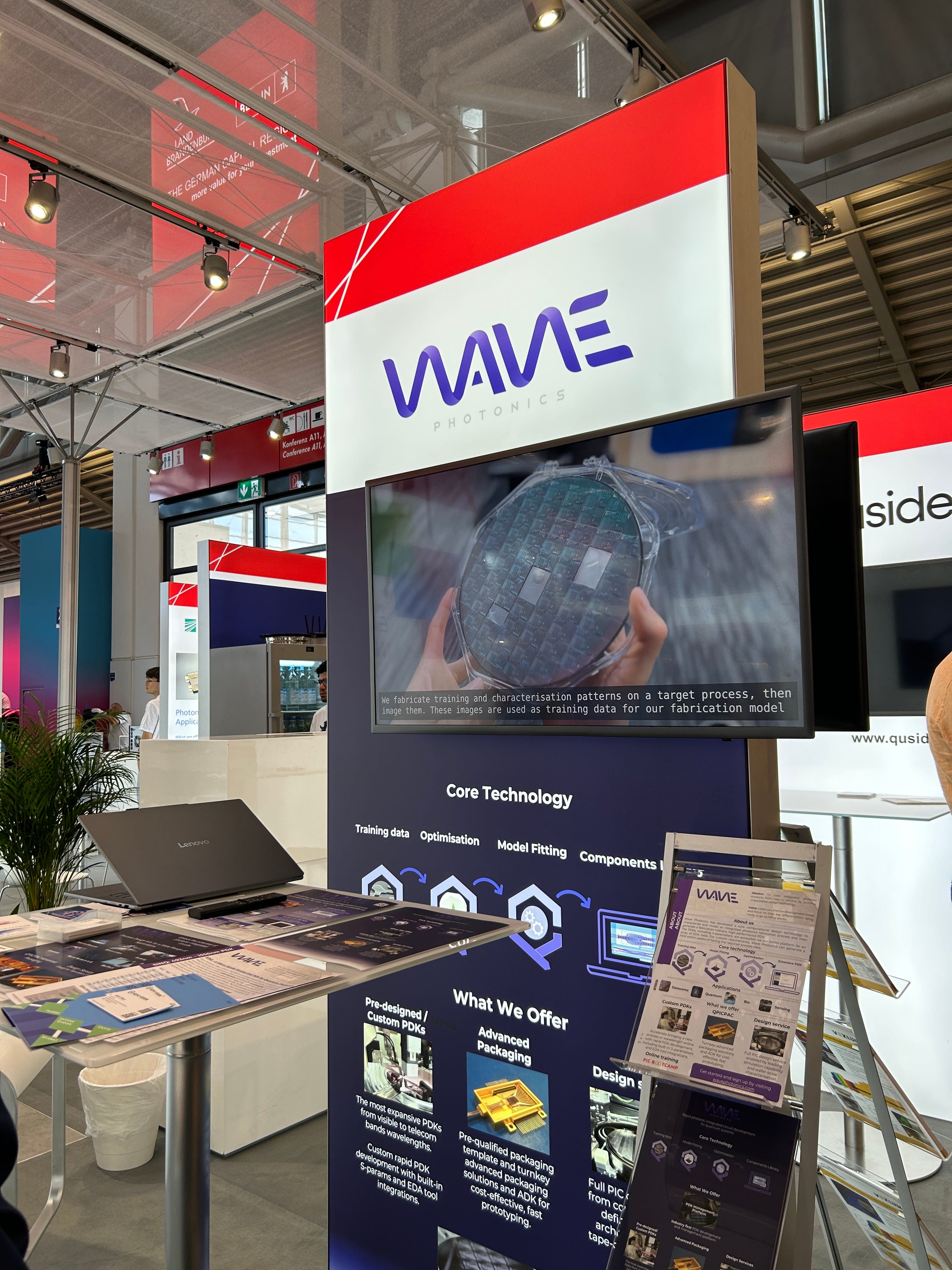
Wave Photonics is a UK-based design company dedicated to bringing photonic products from concept to scalable reality through advanced computational design technologies. Its proprietary platform enables robust fabrication modeling, PDK optimization, and EDA integration, supporting fast, fault-tolerant PIC development.
The company’s flagship platform, SiNQ, delivers a 200 nm silicon nitride PDK covering 493–1550 nm wavelengths. Designed for quantum photonics, it includes over 1,056 components and supports 33 distinct wavelengths, optimized for NV centers, ion sources, and quantum dots. Applications include quantum communication and sensing, using emitters like NV centers, Cr centers, lithium, and rubidium atoms.
Wave Photonics offers:
Custom PDK development
Full-stack PIC design services
Wafer-level characterization
Advanced packaging integration via partners like SENKO and ALTER (QPiCPAC)
The platform is fully compatible with major EDA tools, including Siemens, Cadence, Luceda, and GDS Factory, enabling accelerated development cycles and increased design reusability. For customers requiring custom components, Wave can generate fabrication-ready PDKs within weeks, delivering true design-to-package capability for quantum, biosensing, telecom, and emerging markets.
EPIC: European Photonics Industry Consortium

EPIC (European Photonics Industry Consortium) is a leading global industry association advancing the competitiveness of the European photonics ecosystem. With members from photonic components, systems, manufacturing, and applications, EPIC fosters innovation, business development, and international collaboration.
Core Services:
Technical workshops and international conferences
EU project engagement and B2B matchmaking
Investment support and market insights
Talent and HR matching
Member-to-member networking and thematic working groups
EPIC actively supports cross-sector partnerships and provides market intelligence, access to customer ecosystems, and a platform for high-visibility outreach, making it a cornerstone organization for companies navigating global photonics markets.
OPTICA: Advancing Optics and Photonics Worldwide

Formerly known as OSA, OPTICA is one of the most influential global professional societies in optics and photonics. Rebranded in 2021, OPTICA focuses on interdisciplinary innovation, academic-industry linkage, and international outreach.
Key Missions:
Support cutting-edge R&D in photonics, including quantum technologies, sensing, imaging, energy, and space
Publish top journals such as Optica, Optics Letters, and Applied Optics
Host 40+ global conferences including OFC, CLEO, and Frontiers in Optics
Bridge academia, startups, and industry through forums, grants, and student outreach
Develop global photonics talent through fellowships, mentoring, and education programs
Focus Areas:
Quantum photonics
Silicon photonics & advanced packaging
THz and mid-infrared optics
Sustainable photonic technologies
With over 432,000 members/readers in 100+ countries, OPTICA serves as a crucial force in both scientific progress and industry commercialization. Members include Intel, NVIDIA, NTT, TSMC, Lightmatter, Ayar Labs, and more.
As artificial intelligence and high-speed data processing continue to drive bandwidth and energy efficiency demands in data centers and computing platforms, traditional electrical I/O architectures are reaching their performance limits. Against this backdrop, the LED industry is undergoing a profound transformation—shifting from display and lighting applications toward becoming a core enabler of optical interconnect technologies, particularly in the realm of Chip-to-Chip (C2C) optical links.
Among the leaders in this transition is ams OSRAM, which is actively leveraging its expertise in high-brightness miniaturized LEDs—such as Micro LEDs and VCSELs—to develop photonic I/O modules tailored for AI and HPC architectures. These modules are designed to deliver high-speed, low-power optical sources. In parallel, TSMC plays a pivotal role by providing the silicon photonics platform and advanced packaging capabilities. Through its integration of silicon waveguides, modulators, and photodetectors on 65nm and more advanced CMOS nodes, TSMC enables co-packaging of photonic components with logic chips.

Avicena, a pioneer in precision sensors and silicon photonics modules, is also deeply engaged in the development of actively aligned optical modules, low-latency optical transceivers, and embedded C2C optical channels. The company has entered into several joint development programs (JDPs) with TSMC and ams OSRAM to create a vertically integrated supply chain that spans light sources, modulators, detectors, and ASIC integration.
This collaborative model signals a full-stack transformation “from emitter fabrication to silicon photonic packaging,” breathing new life into traditional LED technologies and laying the foundation for future Co-Packaged Optics (CPO) and Optical I/O (OIO) applications. As the silicon photonics industry advances toward large-scale integration and cost-effective manufacturing, the combined efforts of TSMC, ams OSRAM, and Aceinna are steadily building a next-generation optical interconnect ecosystem—spanning materials, emitters, photonic-electronic integration, and system-level packaging.


Technology Forum Integrated Photonics Applications
DEEPLIGHT: Integrated Soliton-Based Optical Combs for PICs
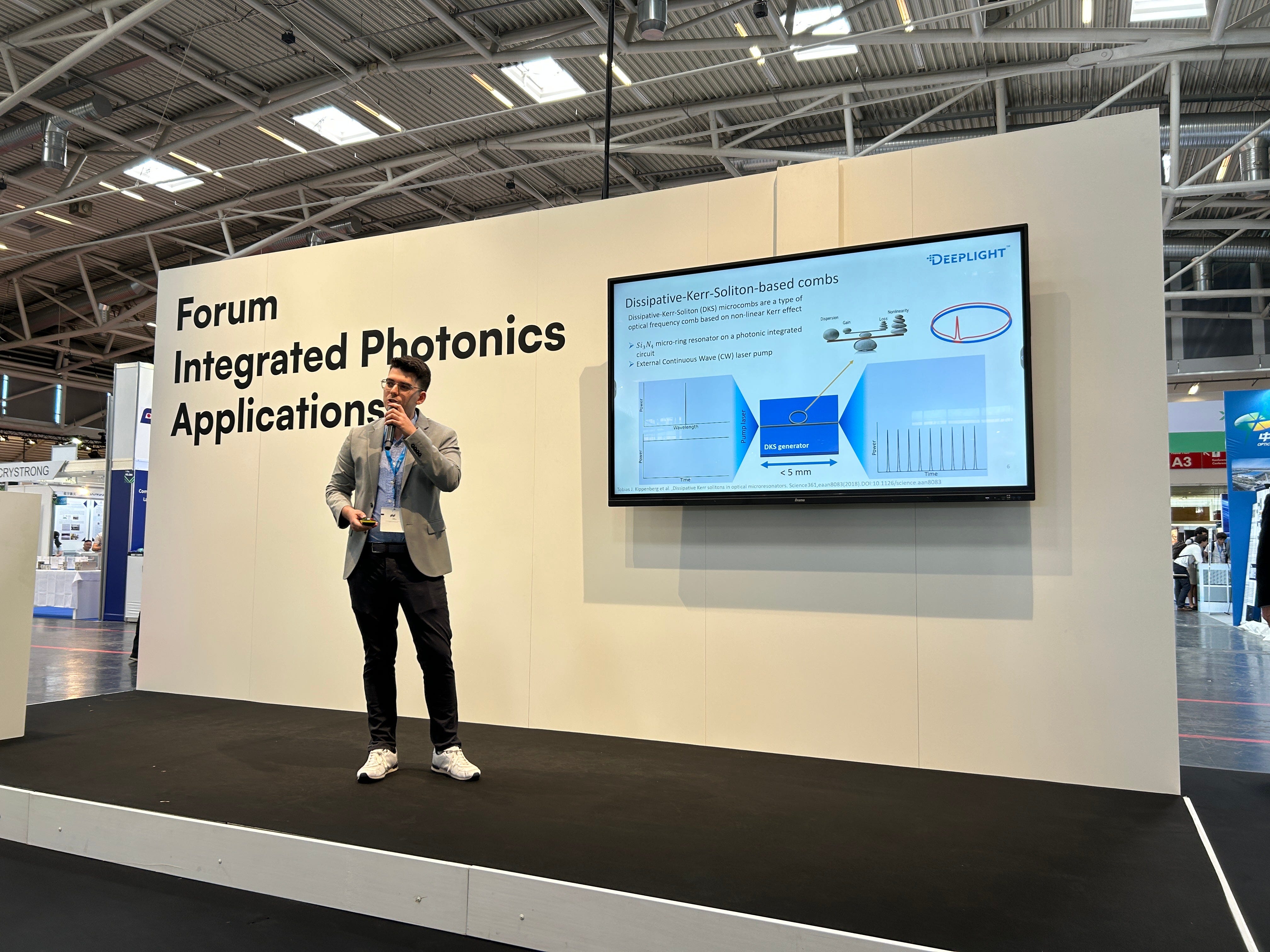
DEEPLIGHT showcased its dissipative Kerr soliton (DKS)-based optical combs, emphasizing superior frequency stability and efficient comb generation for precision timing and PIC system integration. The demonstrated architecture includes pump lasers, filters, comb units, and readout modules, with a strong focus on modular packaging and integration with silicon photonics platforms.

This technology paves the way for integrated optical frequency combs in applications such as LIDAR, quantum computing, spectroscopy, and high-speed communication systems.

PIC Summit Europe 2025
The photonic chip industry is reaching new heights—but scaling production, applications, and investments requires a united effort. As demand surges for high-speed, energy-efficient solutions, the question isn’t if photonic chips will revolutionise industries, but how fast we can make it happen.
At PIC Summit Europe 2025, we bring together an entire ecosystem of designers, foundries, integrators, OEMs, investors, and thought leaders—to tackle the industry’s biggest challenges and opportunities. From advancing manufacturing capacity to expanding market applications and securing funding for growth, this event is where the photonic chip industry aligns its vision for the future.
Why Attend?
Insights straight from the source – Get the latest insights on market and technology developments, helping you navigate the future of PICs with confidence.
Discover real-world applications – Learn which applications are proving most successful, and where the next big opportunities in photonics lie.
Meet key stakeholders – Connect with the most influential players in the industry, from technology leaders to business innovators and investors.
Shape the future of PICs – Gain direction on how to scale your business and technology while aligning with industry-wide efforts. Unlock collaboration opportunities – Whether you're looking for investment, partnerships, or technical cooperation, this is the place to make it happen.
Become a PIC Summit partner?
By partnering with us, you will gain unparalleled visibility, direct access to top decision-makers, and the opportunity to position your solutions at the forefront of the PIC revolution. Join us in fostering innovation, strengthening industry connections, and accelerating the adoption of photonic integrated circuits in real-world applications.
Countries around the world are actively advancing silicon photonics technologies. At the 2025 Laser World of Photonics, both the Netherlands and Canada have established national pavilions.
Netherlands Pavilion
The Dutch photonics organizations PhotonDelta and PhotonicsNL have jointly established the “Netherlands Pavilion” in Hall A2, showcasing an integrated photonics supply chain. The pavilion also hosts networking luncheons and technical forums.

Exhibitors at the NL Pavilion
You can find the NL Pavilion at stand A2.240, located right next to the Integrated Photonics Area at stand A2.250.
Canada Pavilion
The Canadian pavilion features exhibitors including the National Optics Institute (INO), highlighting Canada’s advancements and technologies in photonics.
Industry Insight: Photonics in Canada has tradition and future
More than 400 companies and a good dozen scientific institutions in Canada are involved in photonics. The industry has a long tradition—and a very lively start-up scene. From today's perspective, it is an astonishingly far-sighted article that Alan Baker published in the Canadian Journal of Communication in 1979. The scientist from Toronto Metropolitan University, then known as Ryerson Polytechnical Institute, writes about the potential of fiber optic technology, which he explains in detail: “The fiber itself is a hair-thin, flexible—yet strong glass filament which can…Read more: https://world-of-photonics.com/en/photonics-industry-portal/detail/photonics-in-canada-has-tradition-and-future.html